Deserial – Serial Peripheral Interface (DSPI)
PXN20 Microcontroller Reference Manual, Rev. 1
30-54 Freescale Semiconductor
The time between the negation of the CS at the end of one frame to the assertion of CS at the next frame
is defined by: T
DT
= P
DT
×DT / F
sys,
but delayed until the next active edge of T
SCK
. The gap is only be
whole period of TSCK and the PDT and DT fields of the specific DSPI_CTARn register select the delay
after transfer. Some values are possible.
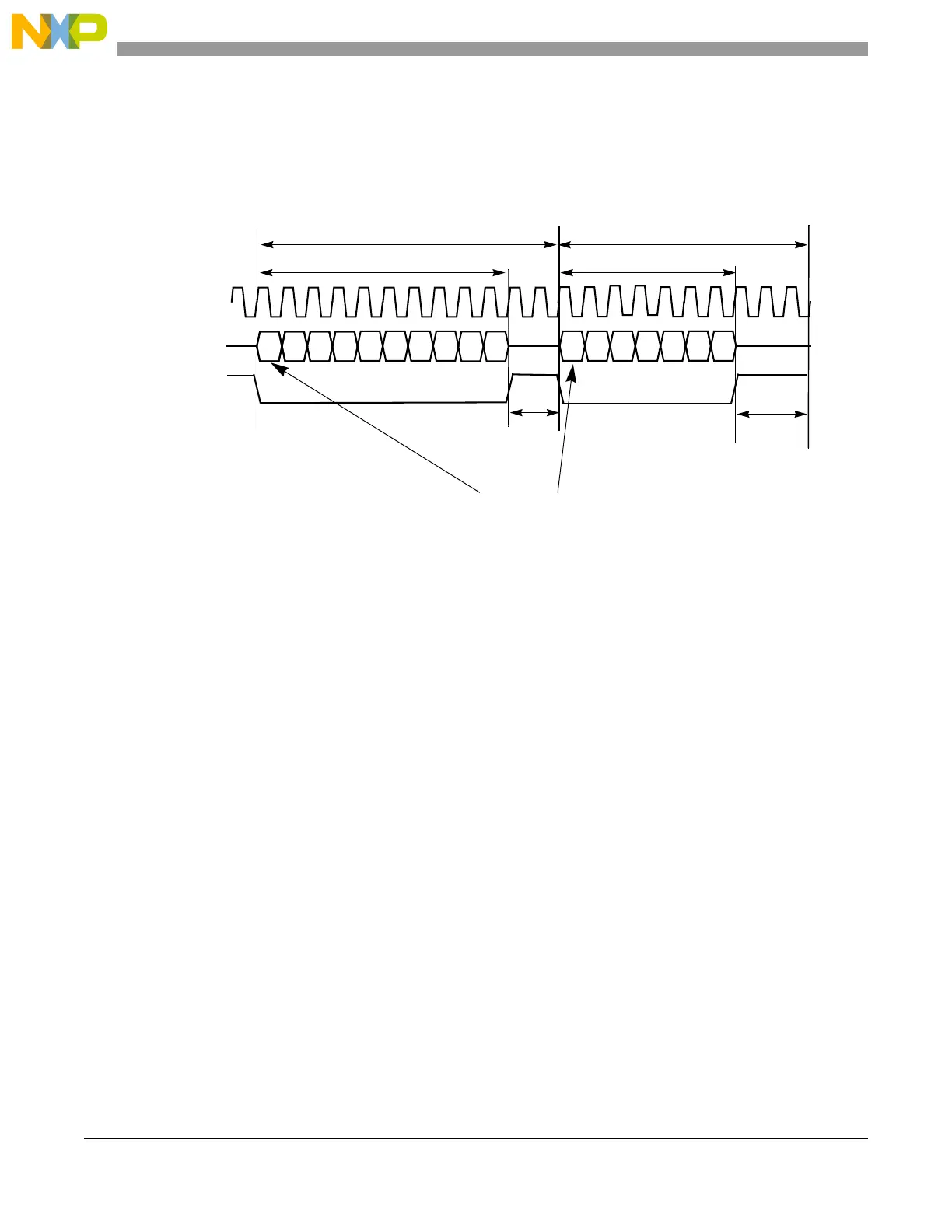
Figure 30-39. TSB Downstream Frame
Figure 30-39 shows the two types of downstream frames used in the TSB configuration, command frame
and data frame. Refer to Section 30.4.10.1, PCS Switch Over Timing, and Section 30.4.10.3, TSB Data
Frame Format, for detailed information. The Command Word can be written by software, and the Data
Word consist of 32-bit words, from the SDR or ASDR registers. Only the downstream frame is supported
in the TSB configuration. The upstream frame can be handled by software using any available serial input.
The selection bit, the start bit for a frame, is not a requirement but could be implemented by software. The
number of frame bits can be in the range of 4 to 32 bits. In this configuration, the least significant bit of a
frame should be transmitted first (LSBFE = 1).
30.4.10.1 PCS Switch Over Timing
When in TSB mode, it is possible to switch the set of PCS signals that are driven during the first part of
the frame to a different set of PCS signals during the second part of the frame. The bit at which this switch
over occurs is contained in the DSICR register.
In order to maximize both the setup and hold time margins on the old and new PCS signals, the timing of
the switch over occurs on the active edge of the master SCK data capture between the last bit of the first
part of the frame and the first bit of the second part of the frame. For example, if the first part of the frame
is 5 bits and the second part of the frame is 10 bits, the PCS signals switch at the active edge of the master
SCK in between bits 5 and 6 of the frame as seen by the slave. The exact timing between the external
signals SCK and PCS signals is not exactly aligned due to routing and pad differences. This approach
ensures that larger/shorter SCK periods result in approximately symmetric increases/decreases of setup
and hold margins on the PCS signals. The setup time for the PCS signals before the first bit of the first part
of the frame and the hold time for the PCS signals after the last bit of the second part of the frame are
t
DT
Data Frame
Invalid
LSB
Active Phase
0
SCK
PCS
Master SOUT
t
DT
= from 1 to (PDT × DT / Fsys) T
SCK
Invalid
Command Frame
t
DT
Command Frame = 0 to 32 bits
LSB
1
Selection Bit
Data Frame = 4 to 32 bits
(CPOL = 0)
Active Phase
 Loading...
