General purpose I/O ports (GPIO) RM0016
106/449 Doc ID 14587 Rev 8
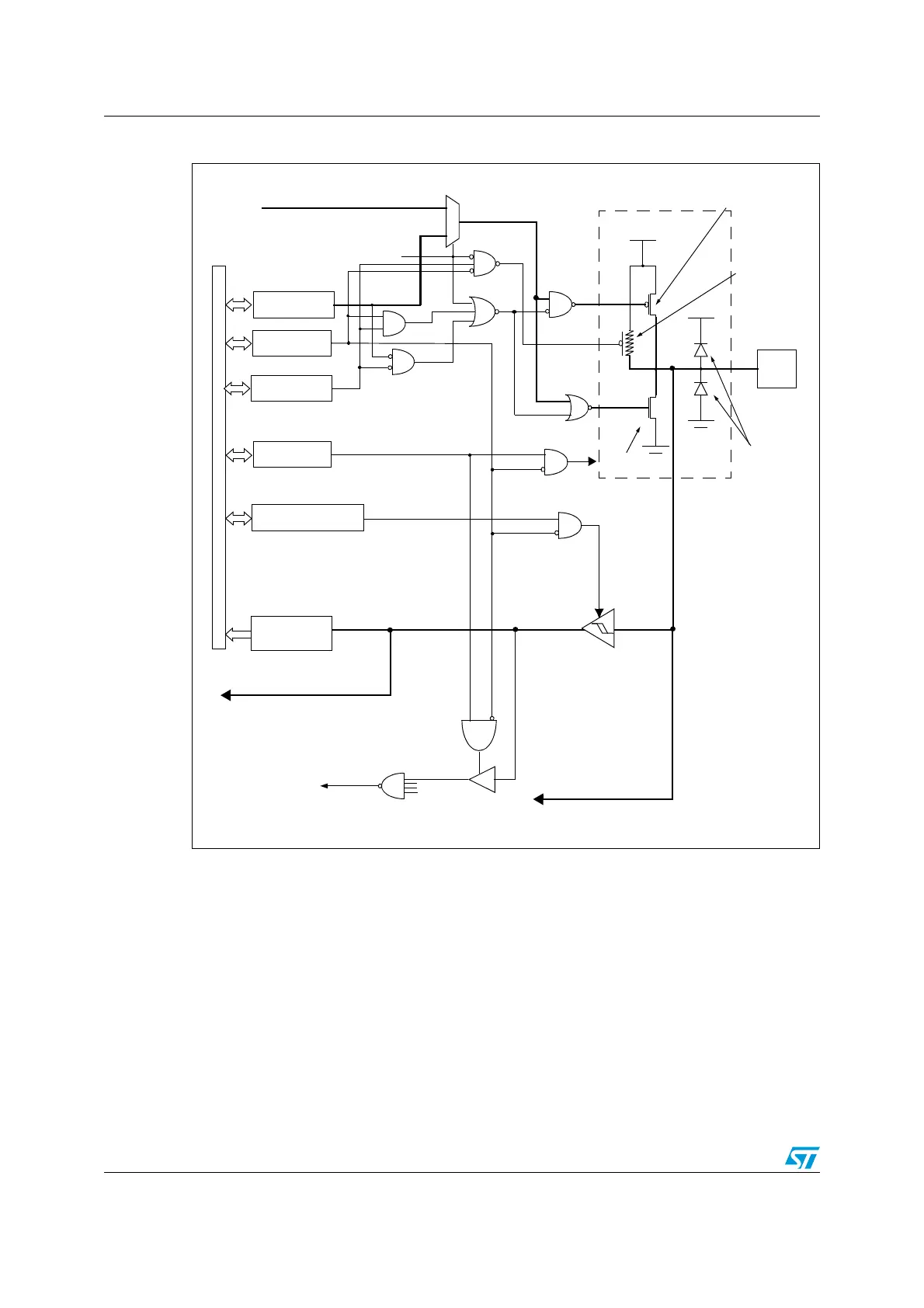
Note: The output stage is disabled when the analog input is selected.
11.3 Port configuration and usage
An output data register (ODR), pin input register (IDR), data direction register (DDR) are
always associated with each port.
The control register 1 (CR1) and control register 2 (CR2) allow input/output options. An I/O
pin is programmed using the corresponding bits in the DDR, ODR, CR1 and CR2 registers.
Bit n in the registers corresponds to pin n of the Port.
The various configurations are summarized in Ta bl e 2 1.
Figure 24. GPIO block diagram
ODR REGISTER
DDR REGISTER
CR1 REGISTER
DATA BUS
PIN
V
DD
ALTERNATE
ENABLE
ALTERNATE
OUTPUT
1
0
PULL-UP
CONDITION
P-BUFFER
(see table below)
N-BUFFER
PULL-UP
(see table below)
ANALOG
INPUT TO A/D CONVERTER
ALTERNATE FUNCTION
INPUT TO ON-CHIP
V
DD
DIODES
(see table below)
FROM
OTHER
BITS
EXTERNAL
TO INTERRUPT
INTERRUPT
CMOS
SCHMITT
TRIGGER
CR2 REGISTER
ADC_TDR REGISTER
PERIPHERAL
CONTROLLER
SLOPE
CONTROL
IDR REGISTER
(Read only)
OUTPUT
INPUT
PAD
PROTECTION
 Loading...


