RM0016 Analog/digital converter (ADC)
Doc ID 14587 Rev 8 425/449
24.11 ADC registers
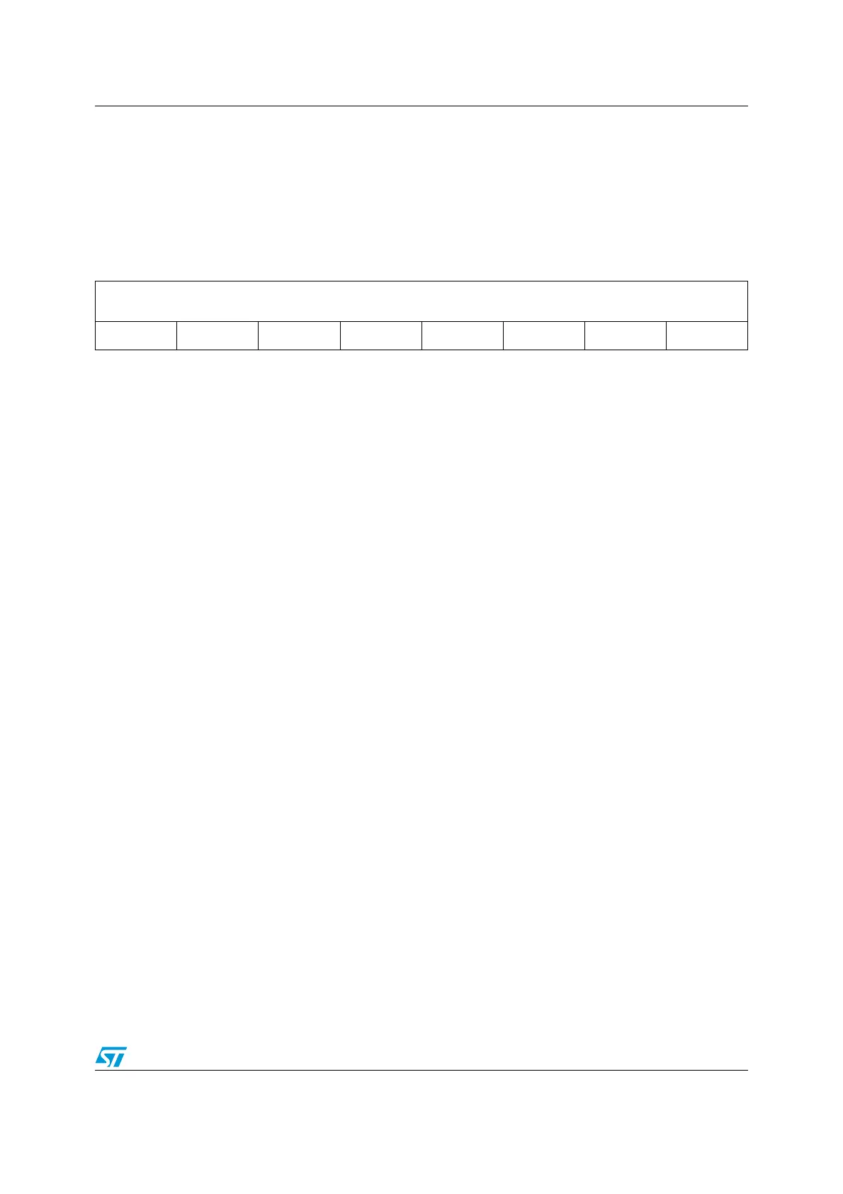
24.11.1 ADC data buffer register x high (ADC_DBxRH) (x=0..7 or 0..9 )
Address offset: 0x00 + 2 * channel number
Reset value: 0x00
Note: Data buffer registers are not available for ADC2. The data buffer size and base address are
device dependent and are specified in the corresponding datasheet. Note that the data
buffer registers and the other ADC registers have different base addresses.
76543210
DBH[7:0]
rrrrrrrr
Bits 7:0 DBH[7:0] Data bits high
These bits are set/reset by hardware and are read only. When the ADC is in
buffered continuous or scan mode, they contain the high part of the converted
data. The data is in right-aligned or left-aligned format depending on the ALIGN
bit.
Left Data Alignment
These bits contain the eight MSB bits of the converted data.
Right Data Alignment
These bits contain the (eight ADC data width) MSB bits of the converted data.
Remaining bits are tied to zero.
See Figure 163.

 Loading...


