16-bit general purpose timers (TIM2, TIM3, TIM5) RM0016
234/449 Doc ID 14587 Rev 8
Channel configured in input
Note: This register is not available in TIM3.
18.6.11 Capture/compare enable register 1 (TIMx_CCER1)
Address offset: 0x08 or 0x0A (TIM2), 0x07 (TIM3), 0x0A (TIM5); for TIM2 address see
Section
Reset value: 0x00
76543210
IC3F[3:0] IC3PSC[1:0] CC3S[1:0]
rw rw rw rw rw
rw
rw rw
Bits 7:4 IC3F[3:0] Input capture 3 filter
Bits 3:2 IC3PSC(1:0]: Input capture 3 prescaler
Bits 1:0 CC3S[1:0]: Capture/compare 3 selection
This bitfield defines the direction of the channel (input/output) as well as the used input.
00: CC3 channel is configured as output
01: CC3 channel is configured as input, IC3 is mapped on TI3FP3
10: Reserved
11: Reserved
Note: CC3S bits are writable only when the channel is off (CC3E = 0 in TIMx_CCER2).
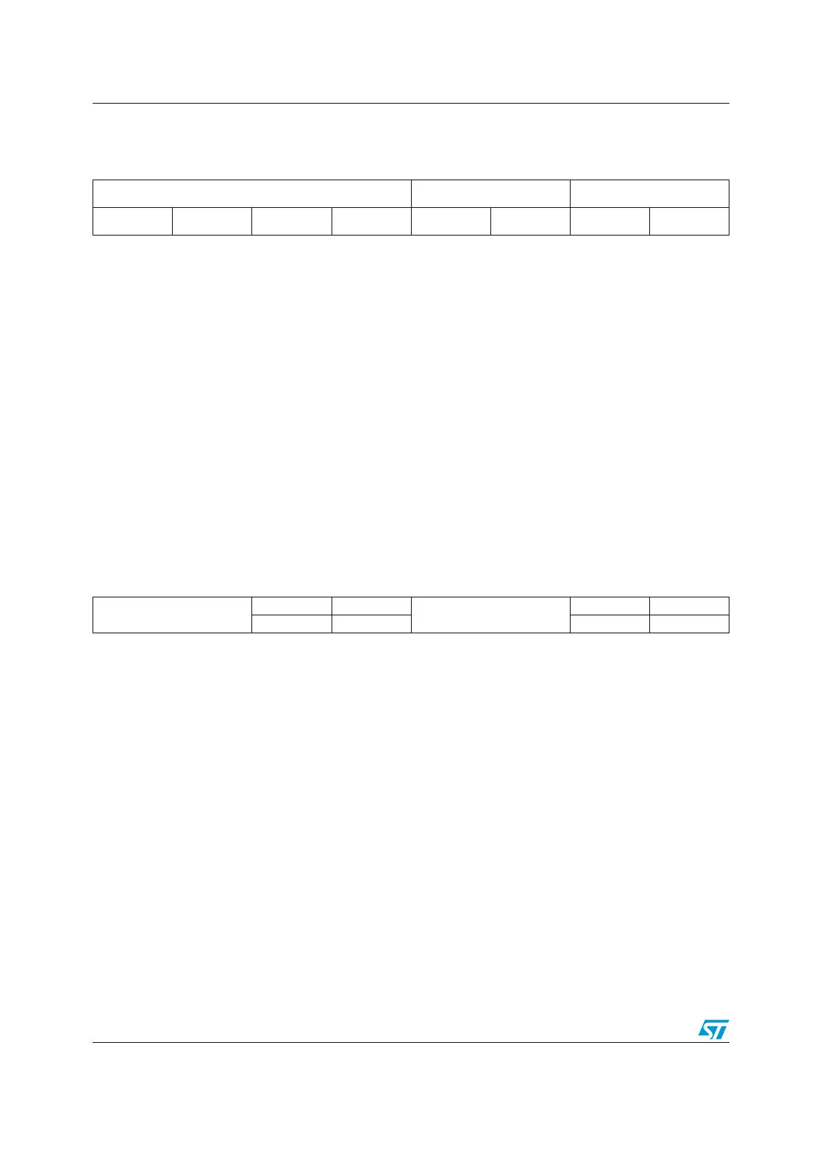
76543210
Reserved
CC2P CC2E
Reserved
CC1P CC1E
rw rw rw rw
Bits 6:7 Reserved
Bit 5 CC2P: Capture/compare 2 output polarity
Refer to CC1P description
Bit 4 CC2E: Capture/compare 2 output enable
Refer to CC1E description.
Bits 2:3 Reserved
Bit 1 CC1P: Capture/compare 1 output polarity
CC1 channel configured as output:
0: OC1 active high
1: OC1 active low
CC1 channel configured as input for capture function (see Figure 64):
0: Capture is done on a rising edge of TI1F or TI2F
1: Capture is done on a falling edge of TI1F or TI2F

 Loading...