RM0016 16-bit advanced control timer (TIM1)
Doc ID 14587 Rev 8 183/449
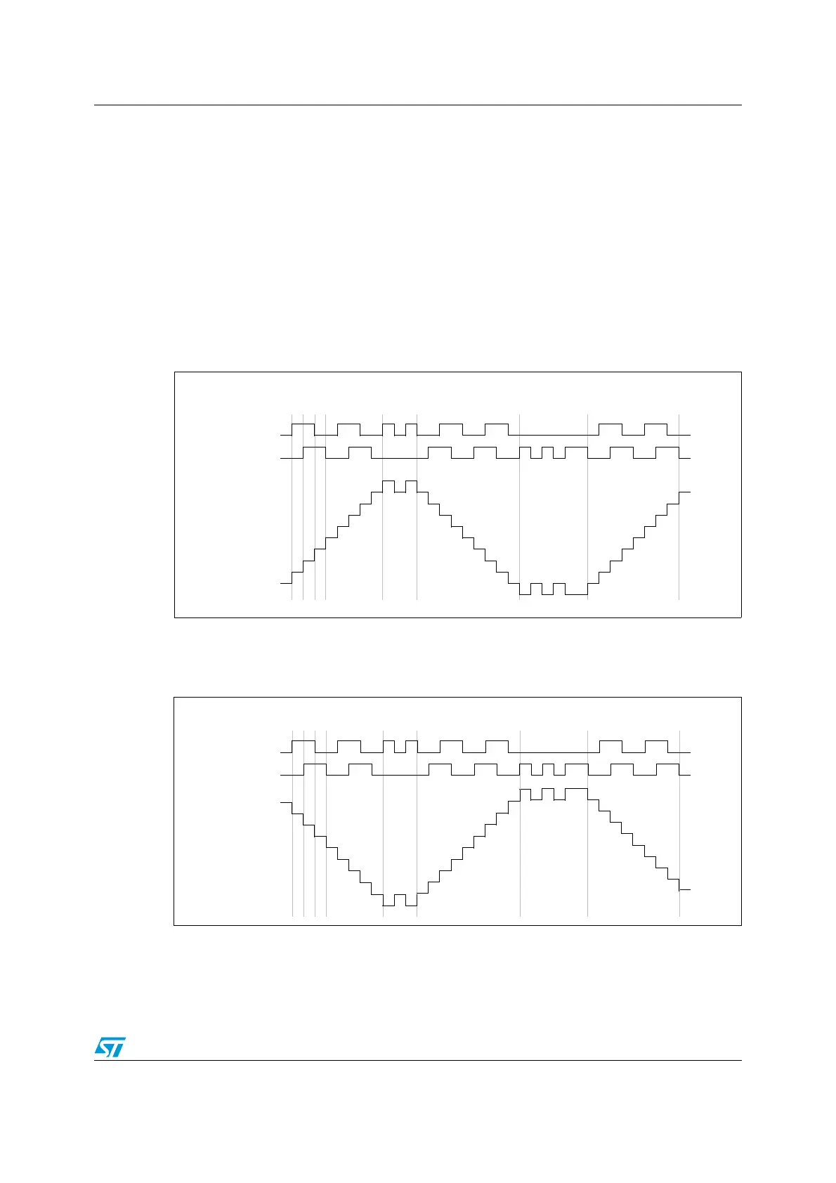
Figure 80 gives an example of counter operation, showing count signal generation and
direction control. It also shows how input jitter is compensated where both edges are
selected. This might occur if the sensor is positioned near one of the switching points. In the
example below, configuration is as follows:
● CC1S = 01 (TIM1_CCMR1 register, IC1 mapped on TI1)
● CC2S = 01 (TIM1_CCMR2 register, IC2 mapped on TI2)
● CC1P = 0 (TIM1_CCER1 register, IC1 non-inverted, IC1=TI1)
● CC2P = 0 (TIM1_CCER2 register, IC2 non-inverted, IC2=TI2)
● SMS = 011 (TIM1_SMCR register, both inputs are active on both rising and falling
edges).
● CEN = 1 (TIM1_CR1 register, counter is enabled)
Figure 80. Example of counter operation in encoder interface mode
Figure 81 gives an example of counter behavior when IC1 polarity is inverted (same
configuration as Figure 80 except that CC1P =1).
Figure 81. Example of encoder interface mode with IC1 polarity inverted
TI1
forward forwardbackwardjitter jitter
up
down up
TI2
COUNTER
TI1
forward forwardbackwardjitter jitter
up
down
TI2
COUNTER
down

 Loading...


