Analog/digital converter (ADC) RM0016
414/449 Doc ID 14587 Rev 8
24.4 ADC pins
24.5 ADC functional description
24.5.1 ADC on-off control
The ADC can be powered-on by setting the ADON bit in the ADC_CR1 register. When the
ADON bit is set for the first time, it wakes up the ADC from power down mode. To start
conversion, set the ADON bit in the ADC_CR1 register with a second write instruction.
At the end of conversion, the ADC remains powered on and you have to set the ADON bit
only once to start the next conversion.
If the ADC is not used for a long time, it is recommended to switch it to power down mode to
decrease power consumption. This is done by clearing the ADON bit.
When the ADC is powered on, the digital input and output stages of the selected channel
are disabled independently on the GPIO pin configuration. It is therefore recommended to
select the analog input channel before powering on the ADC (see Section 24.5.3: Channel
selection).
24.5.2 ADC clock
The clock supplied to the ADC can by a prescaled f
MASTER
clock. The prescaling factor of
the clock depends on the SPSEL[2:0] bits in the ADC_CR1 register.
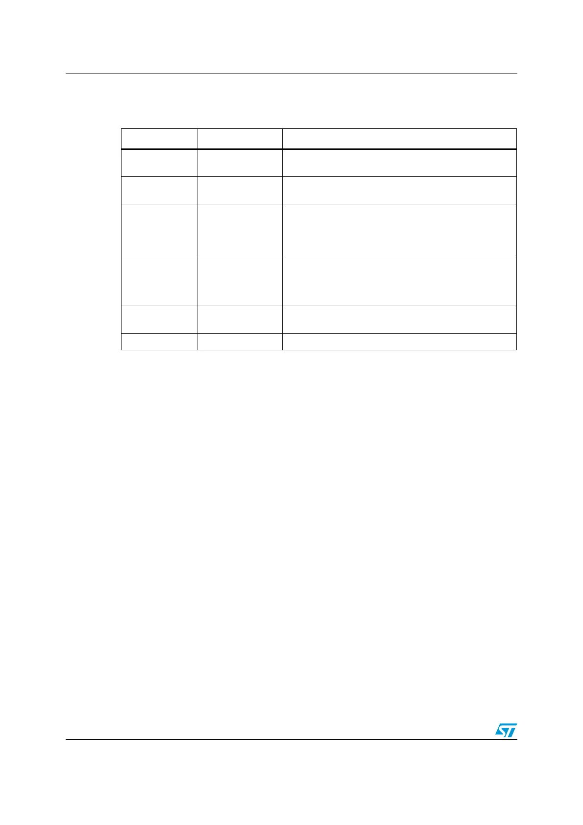
Table 71. ADC pins
Name Signal type Remarks
V
DDA
Input, Analog
supply
Analog power supply. This input is bonded to V
DD
in
devices that have no external V
DDA
pin.
V
SSA
Input, Analog
supply ground
Ground for analog power supply. This input is bonded to
V
SS
in devices that have no external V
SSA
pin.
V
REF-
Input, Analog
Reference negative
The lower/negative reference voltage for the ADC,
ranging from V
SSA
to (V
SSA
+ 500 mV).
This input is bonded to VSSA in devices that have no
external VREF- pin (packages with 48 pins or less)
V
REF+
Input, Analog
Reference positive
The higher/positive reference voltage for the ADC,
ranging from 2.75 V to V
DDA
. This input is bonded to V
DDA
in devices that have no external VREF+ pin (packages with
48 pins or less)
AIN[15:0] Analog input signals
Up to 16 analog input channels, which are converted by
the ADC one at a time.
ADC_ETR Digital input signals External trigger.

 Loading...


