RM0016 16-bit advanced control timer (TIM1)
Doc ID 14587 Rev 8 163/449
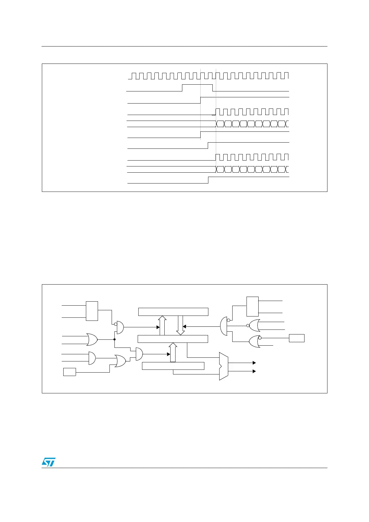
Figure 60. Triggering Timer A and B with Timer A TI1 input
17.5 TIM1 capture/compare channels
The timer I/O pins (TIM1_CCi) can be configured either for input capture or output compare
functions. The choice is made by configuring the CCiS channel selection bits in the
capture/compare channel mode registers (TIM1_CCMRi), where i is the channel number.
Each Capture/Compare channel is built around a capture/compare register (including a
shadow register), an input stage for capture (with digital filter, multiplexing and prescaler)
and an output stage (with comparator and output control).
Figure 61. Capture/compare channel 1 main circuit
00 01
f
MASTER
Timer A-CEN = CNT_EN
Timer A-CNT
Timer A-TI1
Timer A-CK_PSC
02 03 04 05 06 07 08 09
Timer A-TIF
00 01
Timer B-CEN = CNT_EN
Timer B-CNT
Timer B-CK_PSC
02 03 04 05 06 07 08 09
Timer B-TIF
CC1E
Capture/Compare shadow Register
Comparator
Capture/Compare Preload Register
Counter
ic1ps
CC1S[0]
CC1S[1]
capture
input
mode
S
R
Read CCR1H
Read CCR1L
read_in_progress
capture_transfer
CC1S[0]
CC1S[1]
S
R
write CCR1H
write CCR1L
write_in_progress
output
mode
UEV
OC1PE
(from time
compare_transfer
TIMx_CCMR1
OC1PE
base unit)
CNT>CCR1
CNT=CCR1
TIMx_EGR
CC1G

 Loading...


