16-bit general purpose timers (TIM2, TIM3, TIM5) RM0016
232/449 Doc ID 14587 Rev 8
18.6.9 Capture/compare mode register 2 (TIMx_CCMR2)
Note: Refer to Capture/compare mode register 1 (TIMx_CCMR1) on page 230 for details on using
these bits.
Address offset: 0x06 or 0x08 (TIM2), 0x06 (TIM3), 0x08 (TIM5 ); for TIM2 address see
Section
Reset value: 0x00
Channel configured in output
Bits 1:0 CC1S[1:0]: Capture/compare 1 selection
This bitfield defines the direction of the channel (input/output) as well as the used input.
00: CC1 channel is configured as output
01: CC1 channel is configured as input, IC1 is mapped on TI1FP1
10: CC1 channel is configured as input, IC1 is mapped on TI2FP1
11: Reserved
Note: CC1S bits are writable only when the channel is OFF (CC1E = 0 in TIMx_CCER1 and
updated).
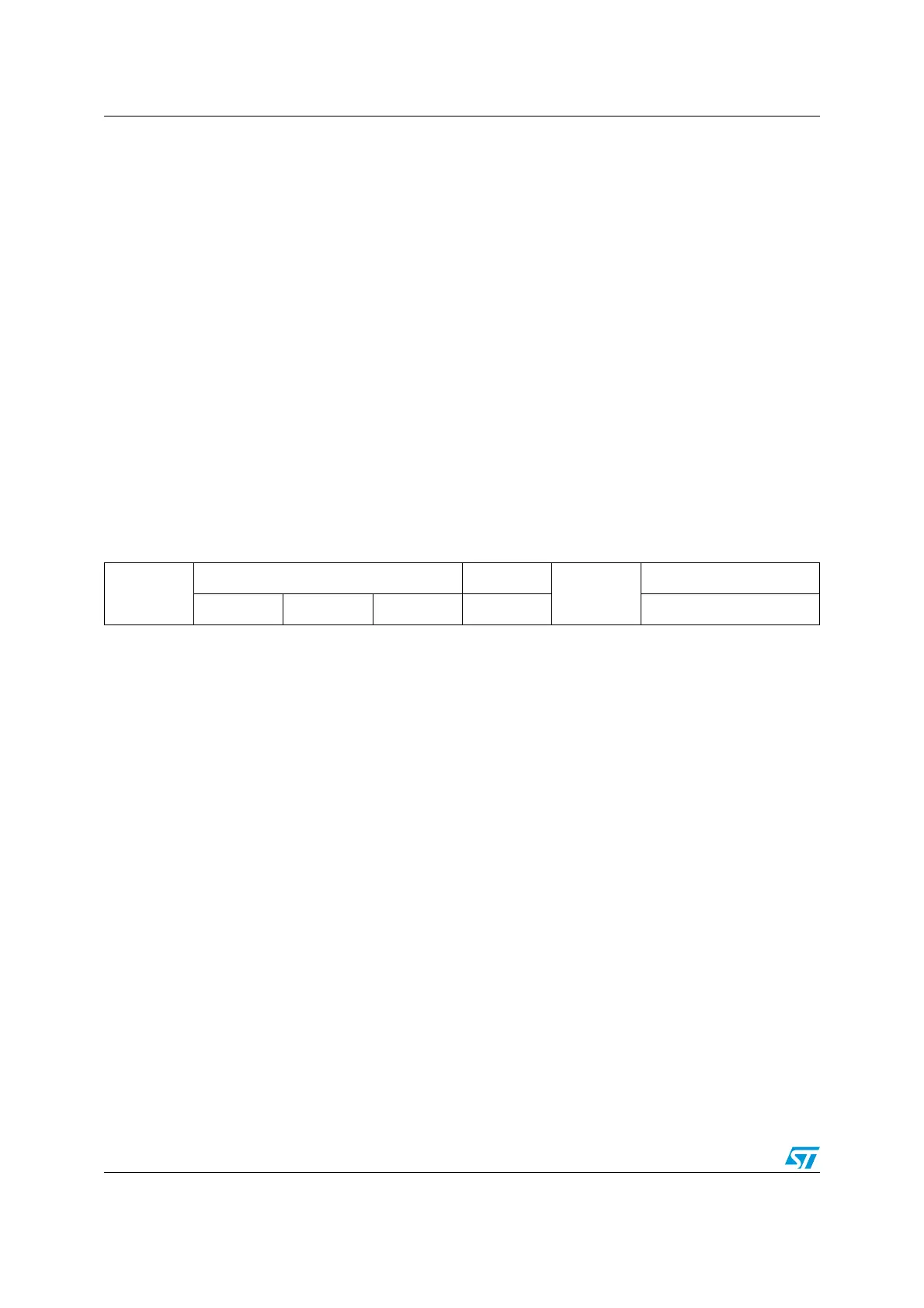
76543210
Reserved
OC2M[2:0] OC2PE
Reserved
CC2S[1:0]
rw rw rw rw rw
Bit 7 Reserved
Bits 6:4 OC2M[2:0]: Output compare 2 mode
Bit 3 OC2PE: Output compare 2 preload enable
Bit 2 Reserved
Bits 1:0 CC2S[1:0]: Capture/compare 2 selection
This bitfield defines the direction of the channel (input/output) as well as the used input.
00: CC2 channel is configured as output
01: CC2 channel is configured as input, IC2 is mapped on TI2FP2
10: CC2 channel is configured as input, IC2 is mapped on TI1FP2
11:CC2 channel is configured as input, IC2 is mapped on TRC. This mode works only if an internal
trigger input is selected through the TS bit (TIM5_SMCR register).
Note: CC2S bits are writable only when the channel is off (CC2E = 0 in TIMx_CCER1).
 Loading...