Inter-integrated circuit (I
2
C) interface RM0016
300/449 Doc ID 14587 Rev 8
21.7.8 Status register 2 (I2C_SR2)
Address offset: 0x08
Reset value: 0x00
6. The ADD10 bit is not set after a NACK reception.
7. The BTF bit is not set after a NACK reception, or in case of an ARLO event.
8. Due to timing constraints, when in standard mode if CCR is less than 9 (i.e. with peripheral clock below 2 MHz) with
f
MASTER
= f
CPU
and the event interrupt disabled, the following procedure must be followed:
modify the reset sequence in order to insert at least 5 cycles between each operations in the flag clearing sequence. For
example, when f
MASTER
= f
CPU
= 1 MHz, use the following sequence to poll the SB bit:
_label_wait: BTJF I2C_SR1,SB,_label_wait
NOP ;
NOP;
NOP ;
NOP
NOP
LD I2C_DR, A ; once executed, the SB bit is then cleared.
9. In slave mode, it is recommended to perform the complete clearing sequence (READ SR1 then READ SR3) after ADDR is
set. Refer to Figure 103: Transfer sequence diagram for slave receiver on page 283.
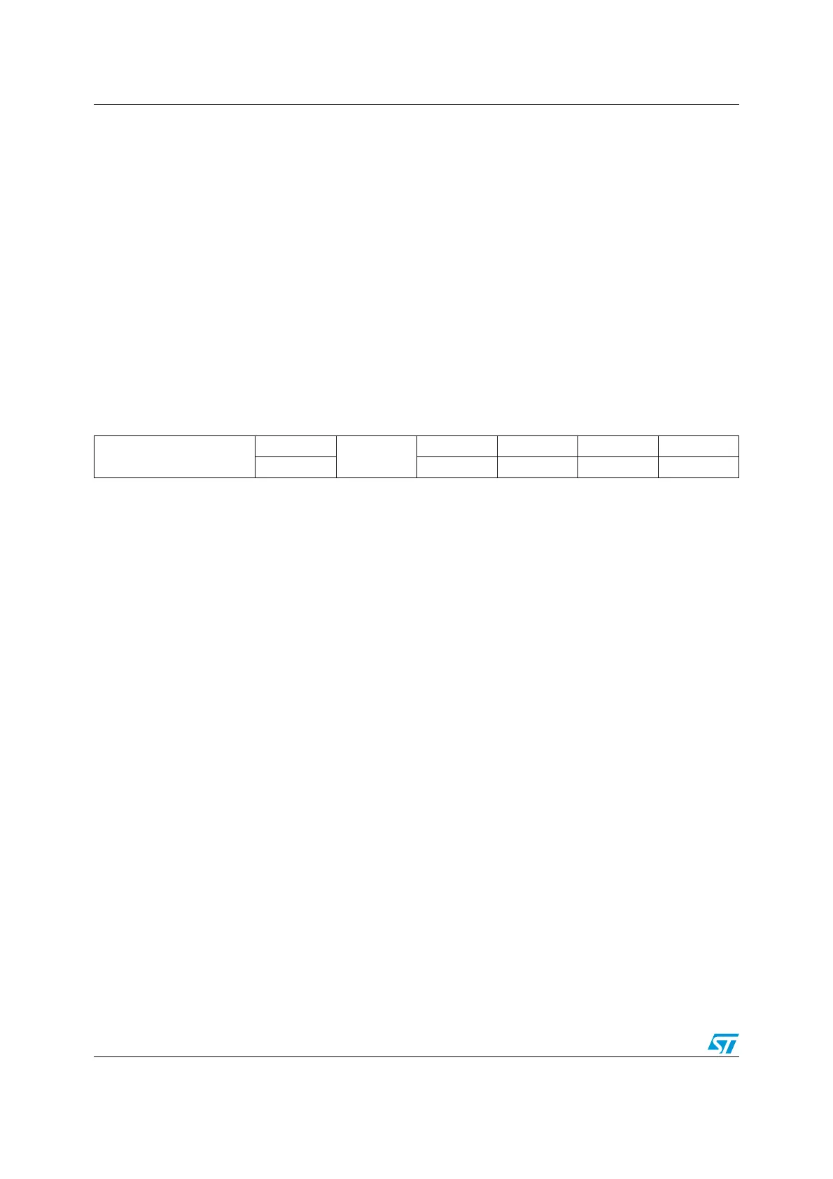
76543210
Reserved
WUFH
Reserved
OVR AF ARLO BERR
rc_w0 rc_w0 rc_w0 rc_w0 rc_w0
Bits 7:6 Reserved
Bit 5 WUFH: Wakeup from Halt
0: no wakeup from Halt mode
1: 7-bit address or header match in Halt mode (slave mode) or Halt entered when in master mode.
Note: This bit is set asynchronously in slave mode (during HALT mode). It is set only if ITEVTEN = 1.
– cleared by software writing 0, or by hardware when PE=0.
Bit 4 Reserved
Bit 3 OVR: Overrun/underrun
0: No overrun/underrun
1: Overrun or underrun
– Set by hardware in slave mode when NOSTRETCH=1 and:
– In reception when a new byte is received (including ACK pulse) and the DR register has not
been read yet. New received byte is lost.
– In transmission when a new byte should be sent and the DR register has not been written
yet. The same byte is sent twice.
Cleared by software writing 0, or by hardware when PE=0.
Note: if the DR write occurs very close to the SCL rising edge, the sent data is unspecified and a hold
timing error occurs.
Bit 2 AF: Acknowledge failure.
0: No acknowledge failure
1: Acknowledge failure
– Set by hardware when no acknowledge is returned.
– Cleared by software writing 0, or by hardware when PE=0.

 Loading...