Inter-integrated circuit (I
2
C) interface RM0016
282/449 Doc ID 14587 Rev 8
Slave transmitter
Following the address reception and after clearing ADDR, the slave sends bytes from the
DR register to the SDA line via the internal shift register.
The slave stretches SCL low until ADDR is cleared and DR filled with the data to be sent
(see Transfer sequencing EV1 EV3 in the following figure).
When the acknowledge pulse is received:
● The TXE bit is set by hardware with an interrupt if the ITEVTEN and the ITBUFEN bits
are set.
If TXE is set and a data was not written in the DR register before the end of the next data
transmission, the BTF bit is set and the interface waits until BTF is cleared, by reading the
SR1 register and then writing to the DR register, stretching SCL low.
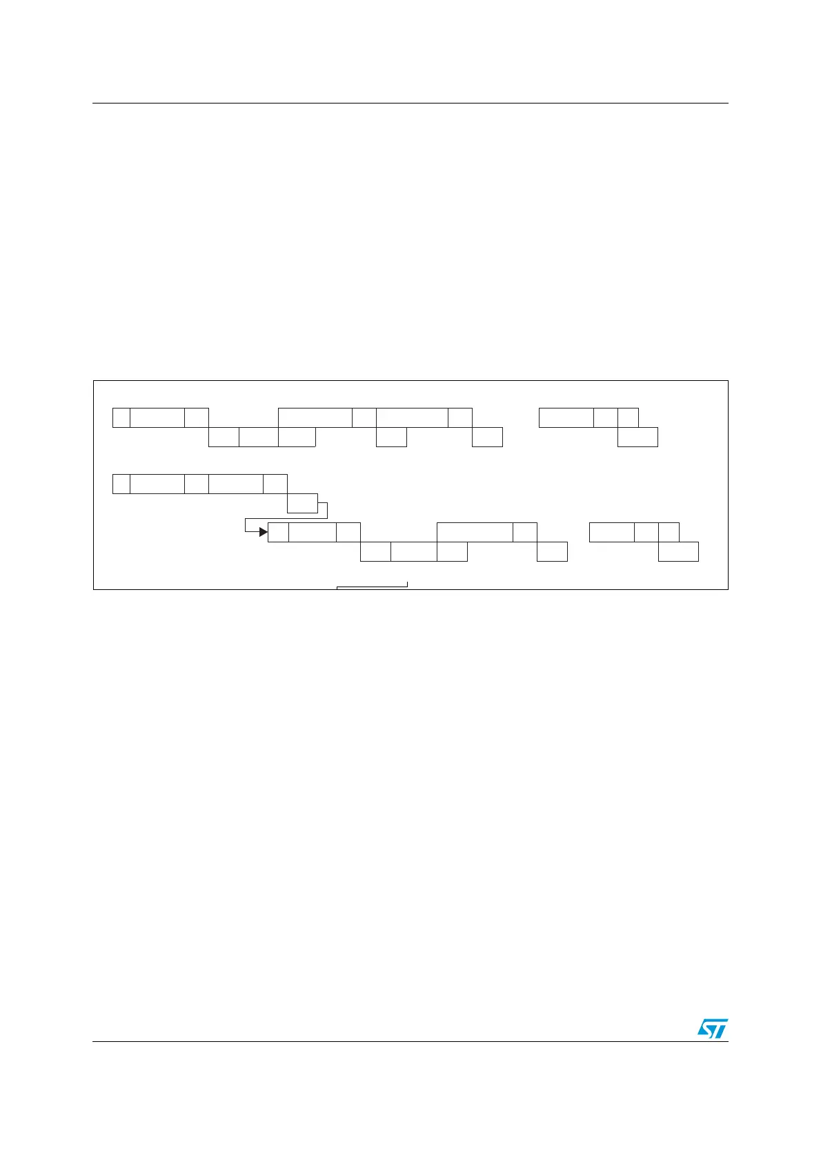
Figure 102. Transfer sequence diagram for slave transmitter
1. Legend:
S= Start, S
r
= Repeated Start, P= Stop, A= Acknowledge, NA= Non-acknowledge, EVx = Event (with interrupt if
ITEVTEN=1)
EV1: ADDR =1, cleared by reading SR1 register followed by reading SR3.
EV3-1: TXE=1, shift register empty, data register empty, write Data1 in DR.
EV3: TXE=1, shift register not empty, data register empty, cleared by writing DR.
EV3-2: AF=1, AF is cleared by writing ‘0’ in AF bit of SR2 register.
2. EV1 and EV3-1 events stretch SCL low until the end of the corresponding software sequence.
3. EV3 software sequence must be performed before the end of the current byte transfer. In case EV3 software sequence can
not be managed before the end of the current byte transfer, it is recommended to use BTF instead of TXE with the
drawback of slowing the communication.
Slave receiver
Following the address reception and after clearing ADDR, the slave receives bytes from the
SDA line into the DR register via the internal shift register. After each byte the interface
generates in sequence:
● An acknowledge pulse if the ACK bit is set
● The RXNE bit is set by hardware and an interrupt is generated if the ITEVTEN and
ITBUFEN bit is set.
If RXNE is set and the data in the DR register is not read before the end of the next data
reception, the BTF bit is set and the interface waits until BTF is cleared, by reading the SR1
register and then reading the DR register, stretching SCL low (see Figure 103).
7-bit slave transmitter
10-bit slave transmitter
S Address AData1A Data2A
.....
DataNNAP
EV1 EV3-1 EV3 EV3 EV3 EV3-2
S Header A Address A
EV1
S
r
Header A Data1A
....
DataNNA
P
EV1 EV3_1 EV3 EV3 EV3-2
ai18209

 Loading...


