RM0016 16-bit advanced control timer (TIM1)
Doc ID 14587 Rev 8 179/449
When a break occurs (selected level on the break input):
● The MOE bit is cleared asynchronously, putting the outputs in inactive state, idle state,
or reset state (selected by the OSSI bit). This happens even if the MCU oscillator is off.
● Each output channel is driven with the level programmed in the OISi bits in the
TIM1_OISR register as soon as MOE = 0. If OSSI = 0, the timer releases the enable
output otherwise the enable output remains high.
● When complementary outputs are implemented:
– The outputs are first put in inactive state (depending on the polarity). This is done
asynchronously so that it works even if no clock is provided to the timer.
– If the timer clock is still present, the deadtime generator is reactivated to drive the
outputs with the level programmed in the OISi and OISi N bits after a deadtime.
Even in this case, OCi and OCi N cannot be driven to their active level together.
Note that because of the resynchronization on MOE, the deadtime duration is a bit
longer than usual (around two 2 ck_tim clock cycles).
● The break status flag (BIF bit in the TIM1_SR1 register) is set. An interrupt can be
generated if the BIE bit in the TIM1_IER register is set.
● If the AOE bit in the TIM1_BKR register is set, the MOE bit is automatically set again at
the next UEV. This can be used to perform a regulation. Otherwise, MOE remains low
until it is written to 1 again. In this case, it can be used for security and the break input
can be connected to an alarm from power drivers, thermal sensors, or any security
components.
Note: The break inputs act on signal level. Thus, the MOE bit cannot be set while the break input
is active (neither automatically nor by software). In the meantime, the status flag BIF cannot
be cleared.
The break can be generated by the break input (BKIN) which has a programmable polarity
and can be enabled or disabled by setting or resetting the BKE bit in the TIM1_BKR register.
In addition to the break inputs and the output management, a write protection has been
implemented inside the break circuit to safeguard the application. It allows the configuration
of several parameters (OCi polarities and state when disabled, OCiM configurations, break
enable, and polarity) to be frozen. Three levels of protection can be selected using the
LOCK bits in the TIM1_BKR register. The LOCK bits can be written only once after an MCU
reset.
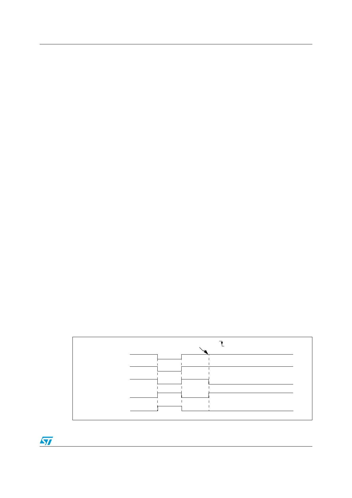
Figure 77 shows an example of the behavior of the outputs in response to a break.
Figure 77. Behavior of outputs in response to a break (channel without
complementary output)
OCiREF
BREAK (MOE
OCi
(
CCi
P=0, OISi=1)
OCi
(
CCi
P=0, OISi=0)
OCi
(
CCi
P=1, OISi=1)
OCi
(
CCi
P=1, OISi=0)
)

 Loading...


