16-bit advanced control timer (TIM1) RM0016
212/449 Doc ID 14587 Rev 8
Note: As the bits AOE, BKP, BKE, OSSR, and OSSI can be write-locked depending on the LOCK
configuration, it is necessary to configure all of them during the first write access to the
TIM1_BKR register.
17.7.31 Deadtime register (TIM1_DTR)
Address offset: 0x1E
Reset value: 0x00
Bits 1:0 LOCK[1:0]: Lock configuration
These bits offer a write protection against software errors.
00: LOCK off - No bits are write protected
01: LOCK level 1 - OISi bit in TIM1_OISR register and BKE/BKP/AOE bits in TIM1_BKR register can
no longer be written.
10: LOCK level 2 - LOCK level 1 + CC polarity bits (CCiP bits in TIM1_CCERi registers, as long as
the related channel is configured in output through the CCiS bits) as well as the OSSR and OSSI
bits can no longer be written.
11: LOCK Level 3 - LOCK level 2 + CC control bits (OCiM and OCiPE bits in TIM1_CCMRi registers,
as long as the related channel is configured in output through the CCiS bits) can no longer be
written.
Note: The LOCK bits can be written only once after reset. Once the TIM1_BKR register has been
written, their content is frozen until the next reset.
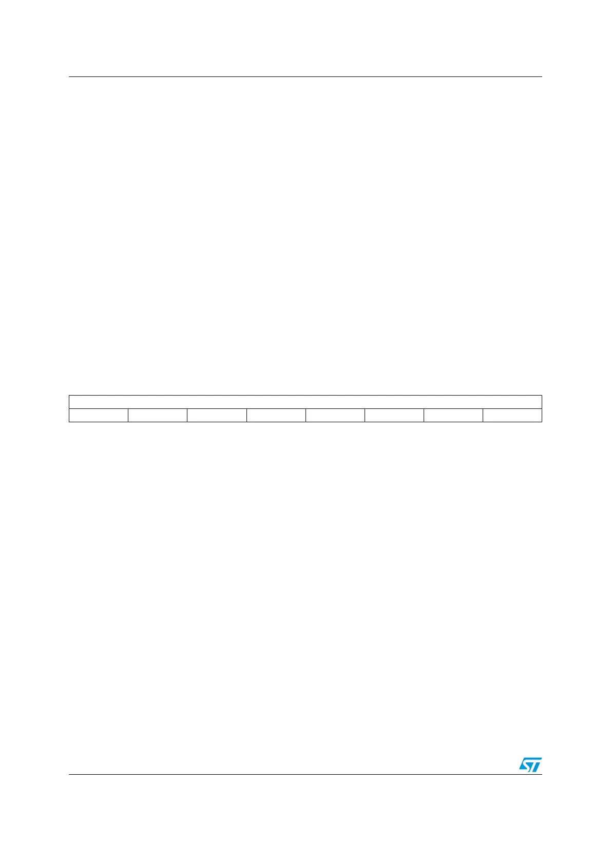
76543210
DTG7:0]
rw rw rw rw rw rw rw rw
Bits 7:0 DTG[7:0]: Deadtime generator set-up
This bitfield defines the duration of the deadtime inserted between the complementary outputs. DT
corresponds to this duration. t
CK_PSC
is the TIM1 clock pulse.
DTG[7:5] = 0xx => DT= DTG[7:0] x t
dtg
with t
dtg
= t
CK_PSC
(f1)
DTG[7:5] = 10x => DT= (64 + DTG[5:0]) x t
dtg
with t
dtg
= 2 x t
CK_PSC
(f2)
DTG[7:5] = 110 => DT = (32 + DTG[4:0]) x t
dtg
with t
dtg
= 8 x t
CK_PSC
(f3)
DTG[7:5] = 111 => DT = (32 + DTG[4:0]) x t
dtg
with t
dtg
= 16 x t
CK_PSC
(f4)
Example
If t
CK_PSC
= 125 ns (8 MHz), deadtime possible values are:
DTG[7:0] = 0 x 0 to 0 x 7F from 0 to 15875 ns in 125 ns steps (refer to f1)
DTG[7:0] = 0 x 80 to 0 x BF from 16 µs to 31750 ns in 250 ns steps (refer to f2)
DTG[7:0] = 0 x C0 to 0 x DF from 32 µs to 63 µs in 1µs steps (refer to f3)
DTG[7:0] = 0 x E0 to 0 x FF from 64 µs to 126 µs in 2 µs steps (refer to f4)
Note: This bitfield can not be modified while LOCK level 1, 2, or 3 have been programmed (LOCK bits
in the TIM1_BKR register).

 Loading...