RM0016 Analog/digital converter (ADC)
Doc ID 14587 Rev 8 431/449
24.11.7 ADC data register high (ADC_DRH)
Address offset: 0x24
Reset value: 0xXX
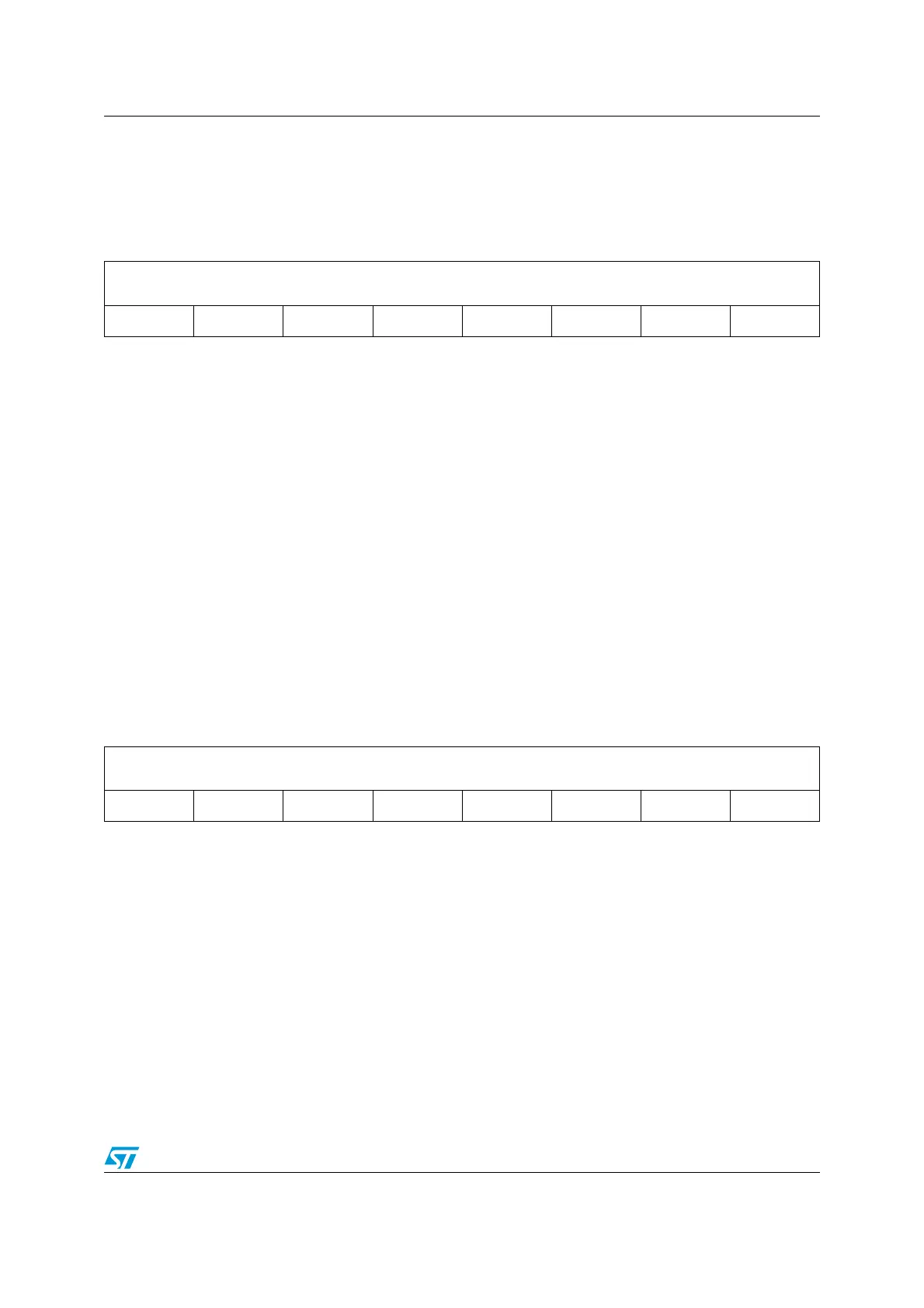
24.11.8 ADC data register low (ADC_DRL)
Address offset: 0x25
Reset value: 0xXX
76543210
DH[7:0]
rrrrrrrr
Bits 7:0 DH[7:0] Data bits high
These bits are set/reset by hardware and are read only. When the ADC is in
single or non-buffered continuous mode, they contain the high part of the
converted data, in right-aligned or left-aligned format depending on the ALIGN
bit.
– Left Data Alignment
These bits contain the 8 MSB bits of the converted data. The MSB must be read
first before reading the LSB (see Section 24.9: Reading the conversion result
and Figure 164.)
– Right Data Alignment
These bits contain the (ADC data width - 8) MSB bits of the converted data.
Remaining bits are tied to zero.
See Figure 163.
76543210
DL[7:0]
rrrrrrrr
Bits 7:0 DL[7:0] Data bits low
These bits are set/reset by hardware and are read only. When the ADC is in
single or non-buffered continuous mode, they contain the low part of the A/D
conversion result, in right-aligned or left-aligned format depending on the
ALIGN bit.
– Left Data Alignment
These bits contain the (ADC data width - 8) LSB bits of the converted data,
remaining bits of the register are tied to zero.
See Figure 164.
– Right Data Alignment
These bits contain the 8 LSB bits of the converted data. The LSB must be read
first before reading the MSB (see Section 24.9: Reading the conversion result
and Figure 163.)

 Loading...


