RM0016 Flash program memory and data EEPROM
Doc ID 14587 Rev 8 55/449
4.8.7 Data EEPROM unprotection key register (FLASH_DUKR)
Address offset: 0x0A
Reset value: 0x00
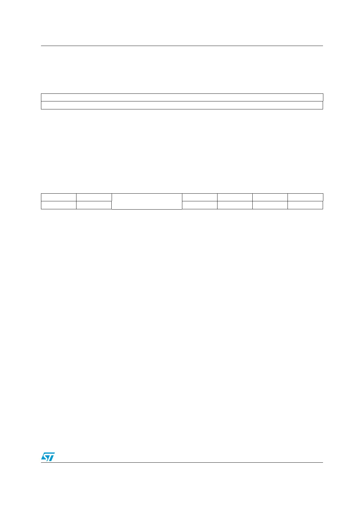
4.8.8 Flash status register (FLASH_IAPSR)
Address offset: 0x05
Reset value: 0x40
76543210
MASS_DATA KEYS
rw
Bits 7:0 DUK[7:0]: Data EEPROM write unlock keys
This byte is written by software (all modes). It returns 0x00 when read.
Refer to Enabling write access to the DATA area on page 45 for the description of main
program area write unprotection mechanism.
76543210
Reserved HVOFF
Reserved
DUL EOP PUL WR_PG_DIS
res. r rc_w0 rc_r rc_w0 rc_r
Bit 7 Reserved.
Bit 6 HVOFF: End of high voltage flag
This bit is set and cleared by hardware.
0: HV ON, start of actual programming
1: HV OFF, end of high voltage
Bits 5:4 Reserved, forced by hardware to 0.
Bit 3 DUL: Data EEPROM area unlocked flag
This bit is set by hardware and cleared by software by programming it to 0.
0: Data EEPROM area write protection enabled
1: Data EEPROM area write protection has been disabled by writing the correct MASS
keys
Bit 2 EOP: End of programming (write or erase operation) flag
This bit is set by hardware. It is cleared by software by reading the register, or when a new
write/erase operation starts.
0: No EOP event occurred
1: An EOP operation occurred. An interrupt is generated if the IE bit is set in the
FLASH_CR1 register.
Bit 1 PUL: Flash Program memory unlocked flag
This bit is set by hardware and cleared by software by programming it to 0.
0: Write protection of main Program area enabled
1: Write protection of main Program area has been disabled by writing the correct MASS
keys.
Bit 0 WR_PG_DIS: Write attempted to protected page flag
This bit is set by hardware and cleared by software by reading the register.
0: No WR_PG_DIS event occurred
1: A write attempt to a write protected page occurred. An interrupt is generated if the IE bit
is set in the FLASH_CR1 register.

 Loading...


