RM0016 Central processing unit (CPU)
Doc ID 14587 Rev 8 27/449
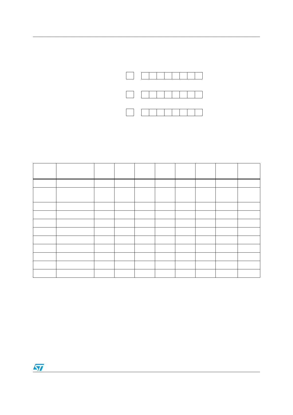
Example: Addition
$B5 + $94 = "C" + $49 = $149
1.2.2 STM8 CPU register map
The CPU registers are mapped in the STM8 address space as shown inTab le 2 . These
registers can only be accessed by the debug module but not by memory access instructions
executed in the core.
1.3 Global configuration register (CFG_GCR)
1.3.1 Activation level
The MCU activation level is configured by programming the AL bit in the CFG_GCR register.
For information on the use of this bit refer to Section 6.4: Activation level/low power mode
control on page 62.
C7 0
0 10110101
C7 0
+0 10010100
C7 0
=1 01001001
Table 2. CPU register map
Address
offset
Register name765432 1 0
0x00 A MSB----- -LSB
0x01 PCE MSB -
-
--- -LSB
0x02 PCH MSB----- -LSB
0x03 PCL MSB----- -LSB
0x04 XH MSB----- -LSB
0x05 XL MSB----- -LSB
0x06 YH MSB----- -LSB
0x07 YL MSB----- -LSB
0x08 SPH MSB----- -LSB
0x09 SPL MSB----- -LSB
0x0A CC V 0 I1 H I0 N Z C

 Loading...


