RM0016 16-bit general purpose timers (TIM2, TIM3, TIM5)
Doc ID 14587 Rev 8 239/449
18.6.22 Capture/compare register 3 high (TIMx_CCR3H)
Address offset: 00x13 or 0x15 (TIM2), 0x15 (TIM5); for TIM2 address see Section
Reset value: 0x00
Note: This register is not available in TIM3.
18.6.23 Capture/compare register 3 low (TIMx_CCR3L)
Address offset: 00x14 or 0x16 (TIM2), 0x16 (TIM5); for TIM2 address see Section
Reset value: 0x00
Note: This register is not available in TIM3.
TIM2/TIM3/TIM5 register map and reset values
In some STM8S and STM8A devices, TIM2 register locations at offset 0x01 and 0x02 are
reserved. In this case the TIM2_IER and subsequent registers in the TIM2 block are offset
by 2 more bytes. Refer to the datasheet for the product-specific register map.
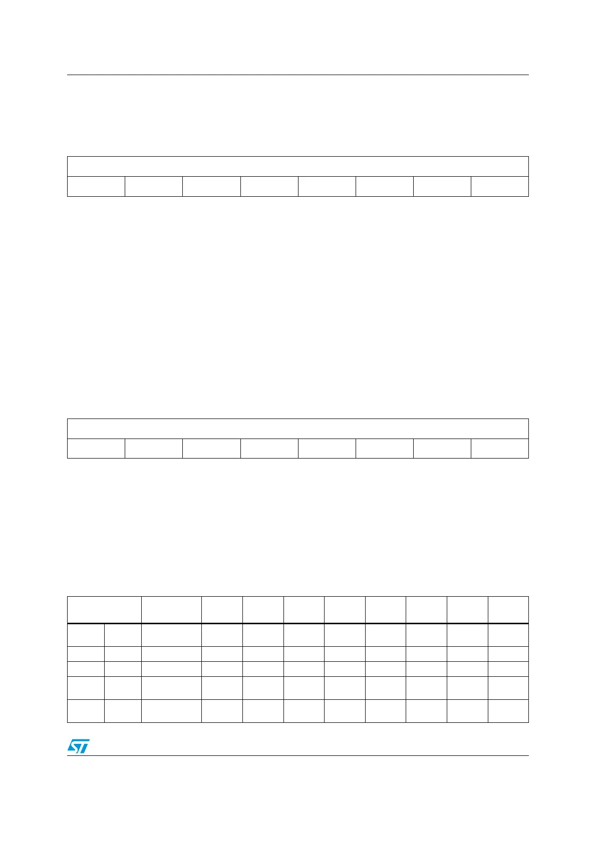
76543210
CCR3[15:8]
rw rw rw rw rw
rw
rw rw
Bits 7:0 CCR3[15:8]: Capture/compare value (MSB)
If the CC3 channel is configured as output (CC3S bits in TIMx_CCMR3 register):
The value of CCR3 is loaded permanently into the actual capture/compare 3 register if the preload
feature is not enabled (OC3PE bit in TIMx_CCMR3). Otherwise, the preload value is copied in the
active capture/compare 3 register when a UEV occurs. The active capture/compare register
contains the value which is compared to the counter register, TIMx_CNT, and signalled on the OC3
output.
If the CC3 channel is configured as input (CC3S bits in TIMx_CCMR3 register):
The value of CCR3 is the counter value transferred by the last input capture 3 event (IC3).
76543210
CCR3[7:0]
rw rw rw rw rw
rw
rw rw
Bits 7:0 CCR3[7:0]: Capture/compare value (LSB)
Table 40. TIM2 register map
Address offset
(product dependent)
Register name76543210
0x00 0x00
TIM2_CR1
Reset value
ARPE
0
-
0
-
0
-
0
OPM
0
URS
0
UDIS
0
CEN
0
- 0x01 Reserved
- 0x02 Reserved
0x01 0x03
TIM2_IER
Reset value
-
0
-
0
-
0
-
0
CC3IE
0
CC2IE
0
CC1IE
0
UIE
0
0x02 0x04
TIM2_SR1
Reset value
-
0
-
0
-
0
-
0
CC3IF
0
CC2IF
0
CC1IF
0
UIF
0

 Loading...


