RM0016 Serial peripheral interface (SPI)
Doc ID 14587 Rev 8 257/449
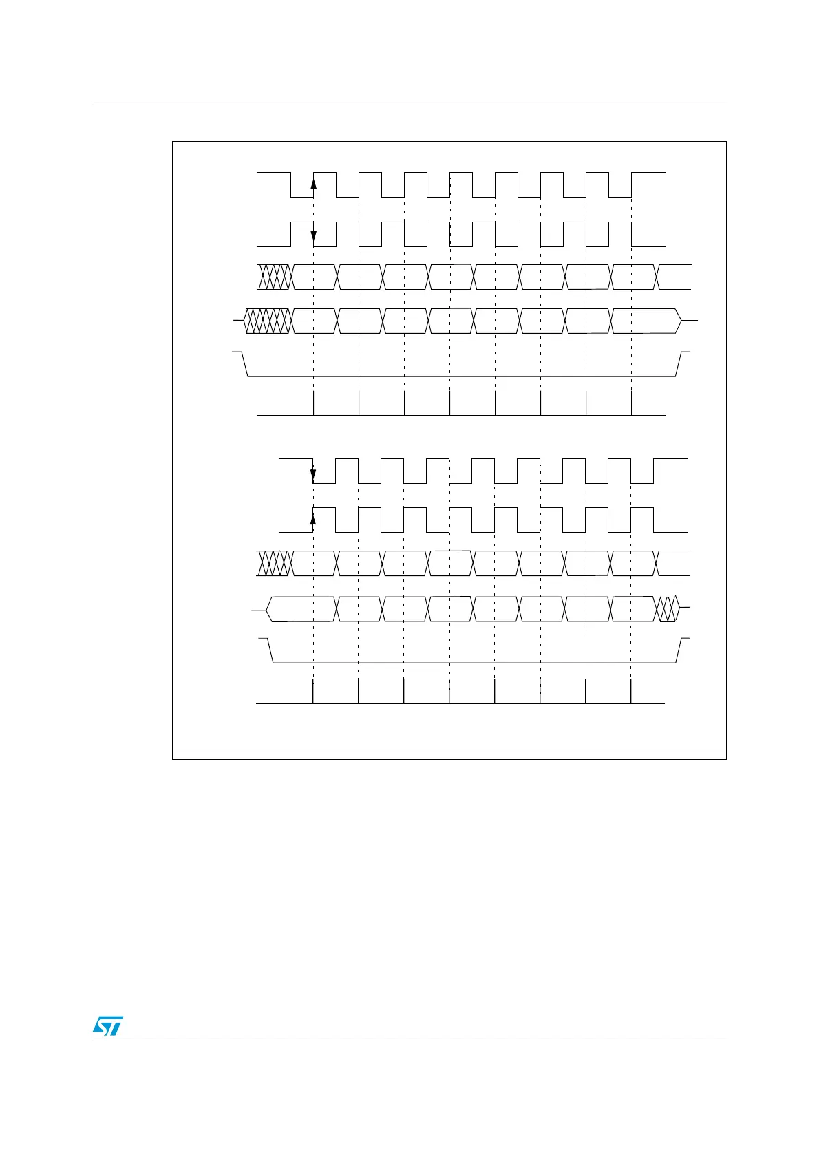
Figure 93. Data clock timing diagram
1. These timings are shown with the LSBFIRST bit reset in the SPI_CR1 register.
Frame format
Data can be shifted out either MSB-first or LSB-first depending on the value of the
LSBFIRST bit in the SPI_CR1 Register.
CPOL = 1
CPOL = 0
MSBit Bit 6 Bit 5
Bit 4 Bit3 Bit 2 Bit 1 LSBit
MSBit Bit 6 Bit 5
Bit 4 Bit3 Bit 2 Bit 1 LSBit
MISO
MOSI
NSS
(to slave)
CAPTURE STROBE
CPHA =1
CPOL = 1
CPOL = 0
MSBit Bit 6 Bit 5
Bit 4 Bit3 Bit 2 Bit 1 LSBit
MSBit Bit 6 Bit 5
Bit 4 Bit3 Bit 2 Bit 1 LSBit
MISO
MOSI
NSS
(to slave)
CAPTURE STROBE
CPHA =0

 Loading...


