General purpose I/O ports (GPIO) RM0016
112/449 Doc ID 14587 Rev 8
11.9.3 Port x data direction register (Px_DDR)
Address offset: 0x02
Reset value: 0x00
11.9.4 Port x control register 1 (Px_CR1)
Address offset: 0x03
Reset value: 0x00 except for PD_CR1 which reset value is 0x02.
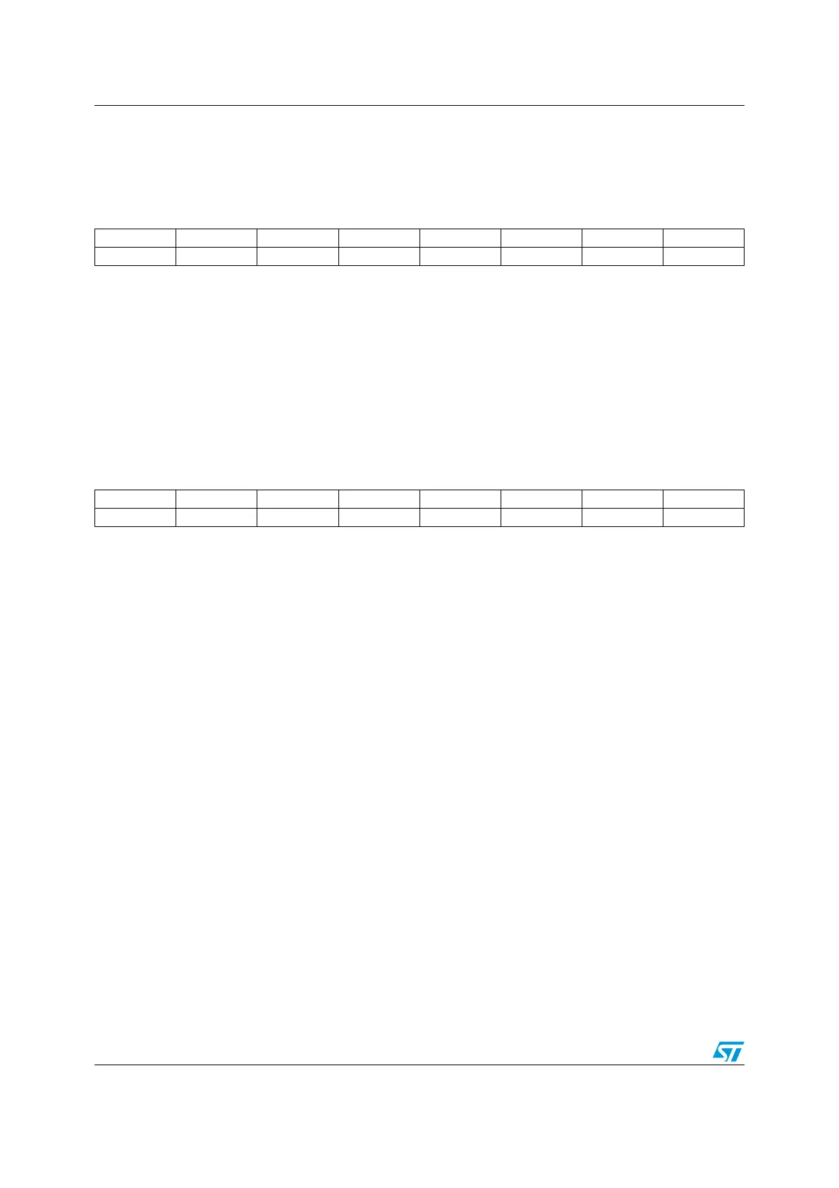
76543210
DDR7 DDR6 DDR5 DDR4 DDR3 DDR2 DDR1 DDR0
rw rw rw rw rw rw rw rw
Bits 7:0 DDR[7:0]: Data direction bits
These bits are set and cleared by software to select input or output mode for a particular pin of a
port.
0: Input mode
1: Output mode
76543210
C17 C16 C15 C14 C13 C12 C11 C10
rw rw rw rw rw rw rw rw
Bits 7:0 C1[7:0]: Control bits
These bits are set and cleared by software. They select different functions in input mode and output
mode (see Ta bl e 2 1).
– In input mode (DDR = 0):
0: Floating input
1: Input with pull-up
– In output mode (DDR = 1):
0: Pseudo open drain
1: Push-pull, slope control for the output depends on the corresponding CR2 bit
Note: This bit has no effect on true open drain ports (refer to pin marked “T” in datasheet pin
description table).

 Loading...


