RM0016 16-bit general purpose timers (TIM2, TIM3, TIM5)
Doc ID 14587 Rev 8 221/449
Output stage
Refer to Section 17.5.4: Output stage on page 168, Section 17.5.5: Forced output mode on
page 169, Section 17.5.7: PWM mode on page 171.
Note: As the clock/trigger controller and the associated TIMx_CR2 and TIMx_SMCR registers are
not implemented in TIM2/TIM3, the one-pulse mode (described in Section 17.5.7: PWM
mode) is not available in TIM2/TIM3.
As shown in Figure 87. TIMx outputs have no deadtime or complementary outputs.
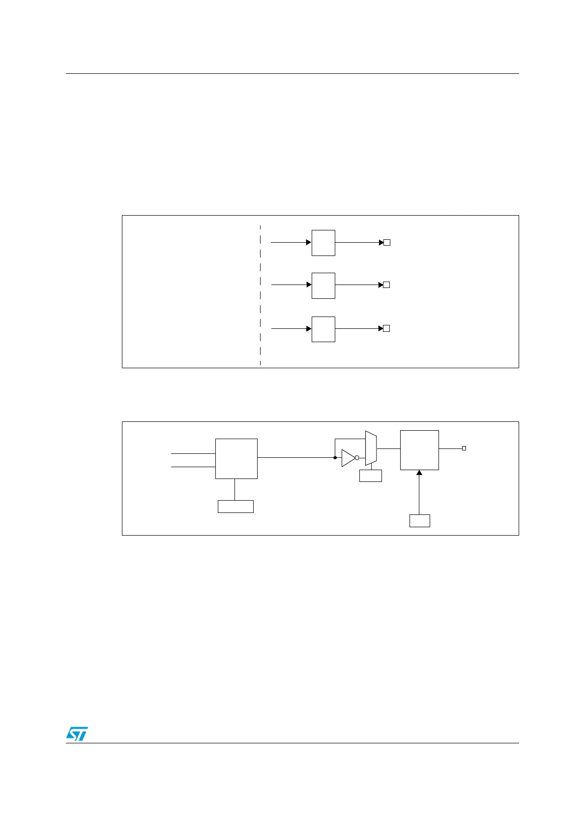
Figure 87. Output stage
The output stage generates an intermediate waveform which is then used for reference:
OCxREF (active high). Polarity acts at the end of the chain (see Figure 88).
Figure 88. Output stage of channel 1
18.5 TIM2/TIM3/TIM5 interrupts
The timers have 4 interrupt request sources:
● Capture/compare 3 interrupt
● Capture/compare 2 interrupt
● Capture/compare 1 interrupt
● Update interrupt
● Trigger interrupt (TIM5 only)
To use the interrupt features, for each interrupt channel used, set the desired CC3IE and/or
CC2IE and/or CC1IE bits in the TIMx_IER register to enable interrupt requests.
OC1REF
OC2REF
OC3REF
output
control
output
control
output
control
TIMx_CH1
OC1
from capture/compare
channels
TIMx_CH2
OC2
TIMx_CH3
OC3
Output Mode
Counter
> CCR1
Counter
= CCR1
Controller
TIMx_CCMR1
OC1M[2:0]
OC1REF
0
1
CC1P
TIMx_CCER1
Output
Enable
Circuit
OC1
CC1E
TIMx_CCER1

 Loading...


