RM0016 Analog/digital converter (ADC)
Doc ID 14587 Rev 8 423/449
24.8 Data alignment
ALIGN bit in the ADC_CR2 register selects the alignment of data stored after conversion.
Data can be aligned in the following ways.
Right Alignment: 8 Least Significant bits are written in the ADC_DL register, then the
remaining Most Significant bits are written in the ADC_DH register. The Least Significant
Byte must be read first followed by the Most Significant Byte. In this case, the LDW
instruction can be used as it has the same reading order.
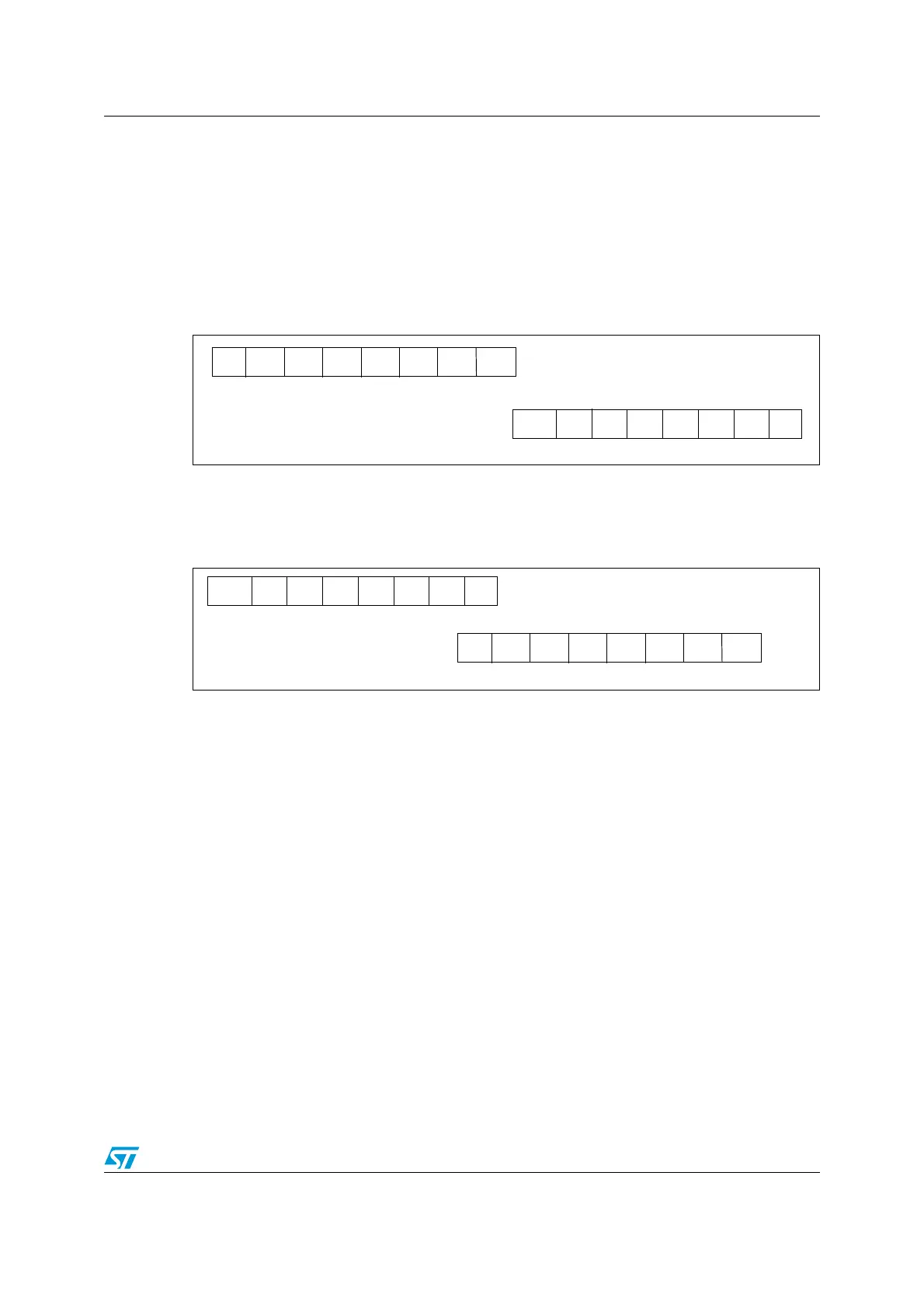
Figure 163. Right alignment of data
Left Alignment: 8 Most Significant bits are written in the ADC_DH register, then the
remaining Least Significant bits are written in the ADC_DL register. The Most Significant
Byte must be read first followed by the Least Significant Byte.
Figure 164. Left alignment of data
24.9 Reading the conversion result
The conversion results from ADC_DRH and ADC_DRL data registers must be read in a
specific order to guarantee data coherency. This order depends on the data alignment (refer
to Section 24.8: Data alignment).
When the ADC1DBxRH and ADC1DBxRL data buffer registers are read (ADC1 only), there
is no internal locking mechanism. Therefore, the user must check the OVR flag in the
ADC_CR3 register after having read the ADC1DBxRH and AD1CDBxRL registers. If the
OVR flag is cleared, this ensures that the values just read from the ADC1DBxRH and
AD1CDBxRL registers are consistent.
Another way to ensure data consistency (with right alignment of data) is to read
ADC1DBxRH and ADC1DBxRL with the following sequence, which must not be interrupted:
ADC_READ:
LDW X,#ADC_DB0RH
CPW X,#ADC_DB0RH
JREQ ADC_END
LDW X,#ADC_DB0RH
ADC_END:
D7
ADC_DRH
ADC_DRL
D8 D9
D6 D5 D4 D3
D2
D1 D0
D9
ADC_DRL
ADC_DRH
D0 D1
D8 D7 D6 D5
D4
D3 D2

 Loading...


