RM0016 General purpose I/O ports (GPIO)
Doc ID 14587 Rev 8 111/449
11.9 GPIO registers
The bit of each port register drives the corresponding pin of the port.
11.9.1 Port x output data register (Px_ODR)
Address offset: 0x00
Reset value: 0x00
11.9.2 Port x pin input register (Px_IDR)
Address offset: 0x01
Reset value: 0xXX
Note: Px_IDR reset value depends on the external circuitry.
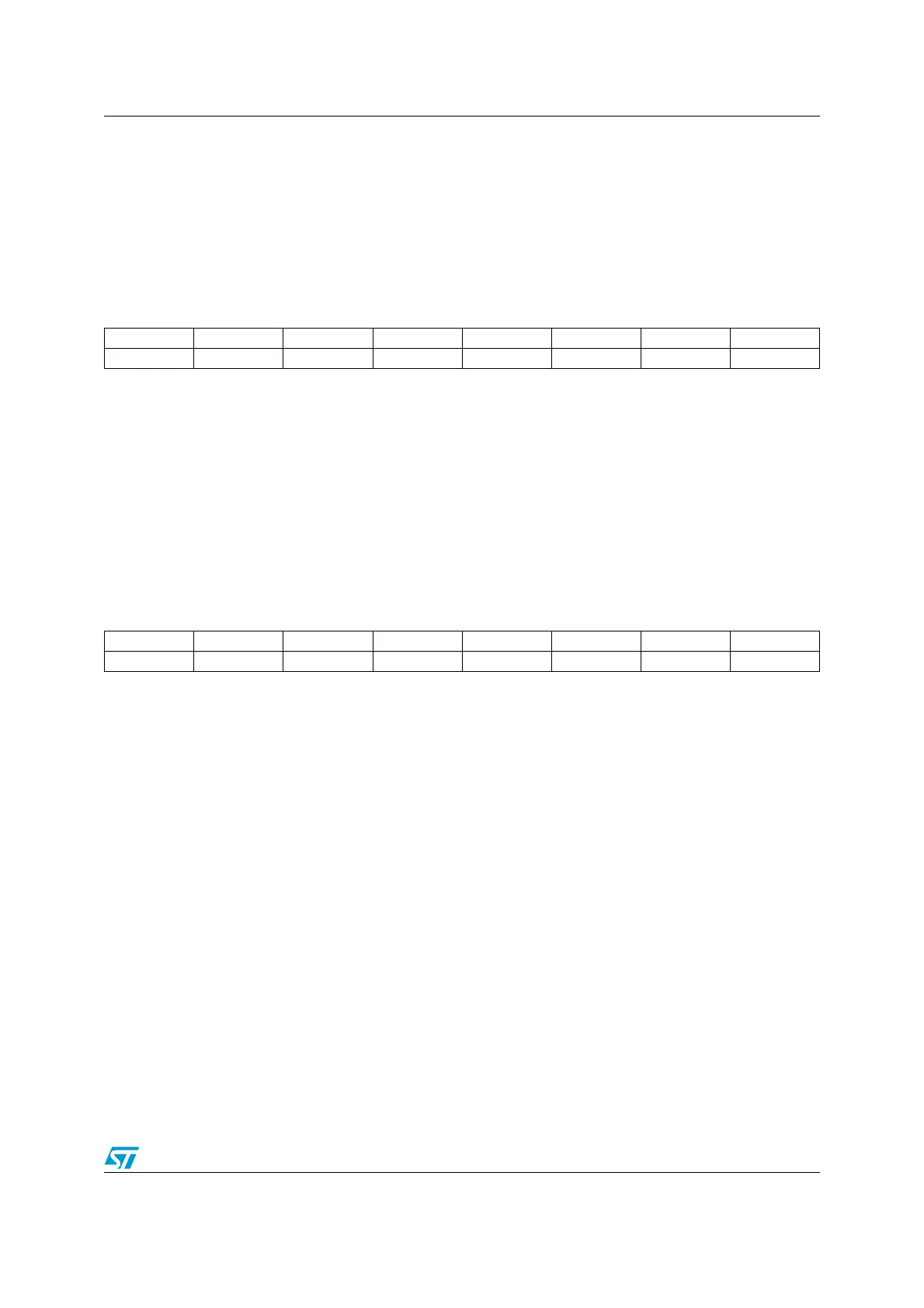
76543210
ODR7 ODR6 ODR5 ODR4 ODR3 ODR2 ODR1 ODR0
rw rw rw rw rw rw rw rw
Bits 7:0 ODR[7:0]: Output data register bits
Writing to the ODR register when in output mode applies a digital value to the I/O through the latch.
Reading the ODR returns the previously latched value in the register.
In Input mode, writing in the ODR register, latches the value in the register but does not change the
pin state. The ODR register is always cleared after reset. Bit read-modify-write instructions (BSET,
BRST) can be used on the DR register to drive an individual pin without affecting the others.
76543210
IDR7 IDR6 IDR5 IDR4 IDR3 IDR2 IDR1 IDR0
rrrrrrrr
Bits 7:0 IDR[7:0]: Pin input values
The pin register can be used to read the pin value irrespective of whether port is in input or output
mode. This register is read-only.
0: Low logic level
1: High logic level

 Loading...


