RM0016 Revision history
Doc ID 14587 Rev 8 445/449
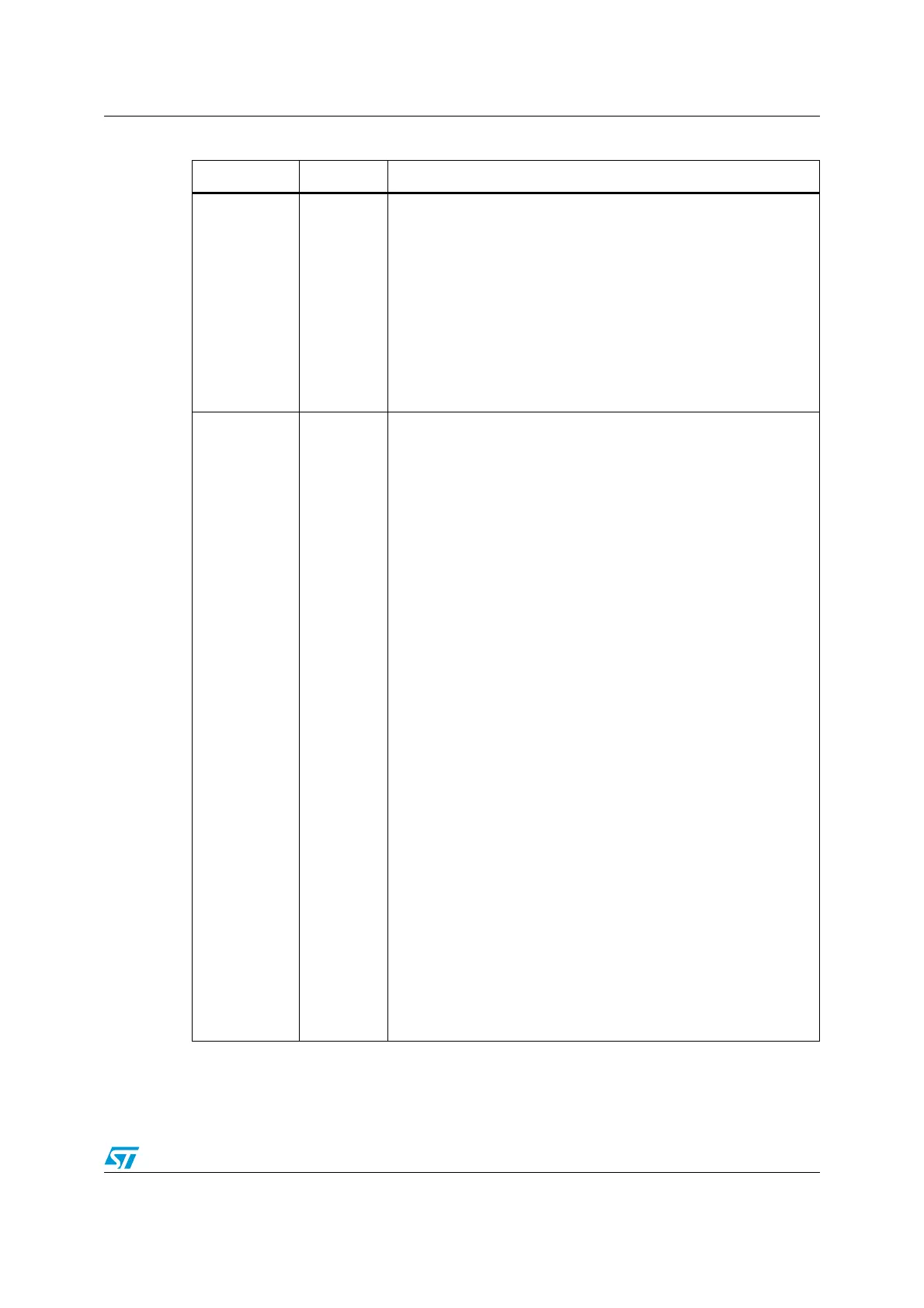
31-Jan-2011 7(continued)
Section 23: Controller area network (beCAN):
– Modified f
CANEXT
upper limit in Section 23.9: Clock system.
– SLEEP and AWUM bit description updated in Section 23.11.1:
CAN master control register (CAN_MCR)
– External beCAN clock source (f
CANEXT
) removed together with bit
CLKS of CAN_BTR2 register.
– Removed CAN register CLK_CANCCR.
Section 24: Analog/digital converter (ADC):
– Updated address offset for ADC _CSR to ADC_AWCRL.
– Added AIN12 pin and Note 1 in Figure 158: ADC1 block diagram,
and note related to AIN12 in Section 24.5.4: Conversion modes.
15-Dec-2011 8
Added value line STM8S devices on page 1
Modified Section 4.4.1: STM8S and STM8A memory organization on
page 36
Modified Section 6.6: External interrupts on page 65
Modified TLIS bit description in Section 6.9.4: External interrupt
control register 1 (EXTI_CR2) on page 70
Modified Figure 20: Clock tree on page 78.
Modiifed HSE oscillator in quartz crystal configuration in Section 9.6:
Clock security system (CSS) on page 87
Removed one sentence in Section 11.8.1: Alternate function output
on page 109.
Modified Timeout period on page 123
Modified Figure 101: I2C block diagram on page 280 (SMBA pin
removed)
Replaced SYSCLK with f
CPU
in Section 15: Window watchdog
(WWDG) on page 126.
Modified Section 15.7: Using Halt mode with the WWDG
(WWDGHALT option) on page 130
Removed note 1 below Figure 101: I2C block diagram on page 280
Added one note in Section : Output stage
Added one note to OPM bit description in Section 18.6.1: Control
register 1 (TIMx_CR1)
Note added below Section 21.7.9: Status register 3 (I2C_SR3) on
page 301
Modified title of Table 55: UART receiver tolerance when
UART_DIV[3:0] is zero on page 322 and Table 56: UART receiver’s
tolerance when UART_DIV[3:0] is different from zero on page 323
Modified RWU bit description in Section 22.7.6: Control register 2
(UART_CR2) on page 352
Modified Section 23.4.2: Normal mode on page 366
Added note to FE bit description in Section 22.7.1: Status register
(UART_SR) on page 348
Modified Section 24.9: Reading the conversion result on page 423
and Section 24.11.2: ADC data buffer register x low (ADC_DBxRL)
(x=or 0..7 or 0..9) (DBL[7:0] instead of DB[7:0])
Table 78. Document revision history (continued)
Date Revision Changes

 Loading...