LH79524/LH79525 User’s Guide Color Liquid Crystal Display Controller
Version 1.0 4-13
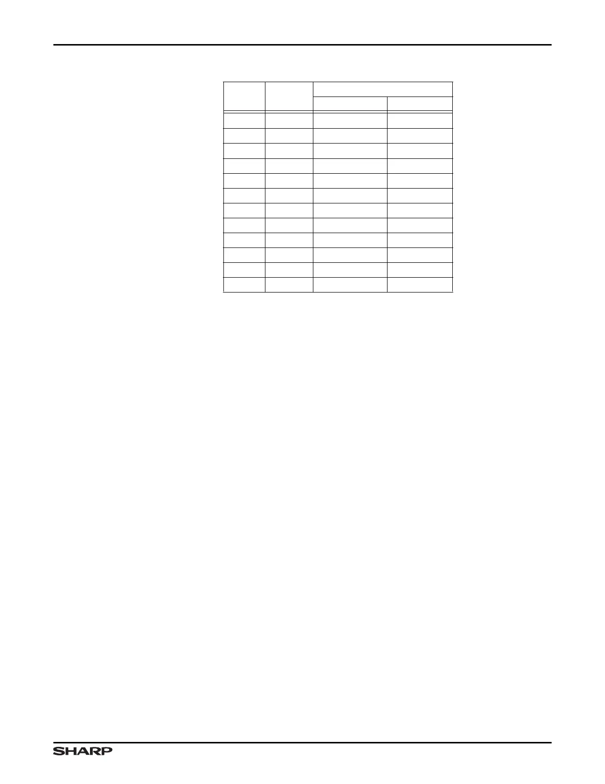
NOTES:
‘X’ is Don’t Care.
‘MLSTNx’ = Mono Lower panel STN data bit ‘x’
‘MUSTNx’ = Mono Upper panel STN data bit ‘x’
‘CLSTNx’ = Color Lower panel STN data bit ‘x’
‘CUSTNx’ = Color Upper panel STN data bit ‘x’
4.3.8 LCD Interface Timing Signals
LCD interface timing signals are categorized as either horizontal or vertical timing signals.
These signals are created by the CLCDC, optionally modified by the ALI, and applied
directly to an external LCD panel with no additional external hardware required, except for
Continuous Grain Silicon (CGS) panels.
4.3.8.1 LCD Horizontal Timing Signals
The horizontal components of LCD timing describe the process of writing one line of LCD
data to a LCD panel and include programmable delays before and after the data is written
to the panel. A line of data is composed of all pixel information for one displayed line. See
Section 4.6 for timing diagrams.
Table 4-11. LH79525 LCD Data Multiplexing
PIN NO.
PIN NAME
STN MONO 4-BIT
SINGLE PANEL DUAL PANEL
145 LCDVD11 MUSTN1 MUSTN1
146 LCDVD10 MUSTN0 MUSTN0
147 LCDVD9
149 LCDVD8
151 LCDVD7 MLSTN3
153 LCDVD6 MLSTN2
154 LCDVD5 MLSTN1
155 LCDVD4 MLSTN0
156 LCDVD3
157 LCDVD2
158 LCDVD1 MUSTN3 MUSTN3
159 LCDVD0 MUSTN2 MUSTN2