Overview LH79524/LH79525 User’s Guide
1-8 Version 1.0
1.4 Reset Strategy
Two external resets, nRESETIN, and nTRST, are used for the LH79524/LH79525. If
nRESETIN is asserted, all internal registers EXCEPT the JTAG circuitry within the
device are set to their default state. The nRESETIN signal should be held LOW for the
crystal stabilization time + 200
μs (the time varies depending on crystal used) during
power-up. If nTRST is asserted, only the JTAG circuitry is set to its default state.
There are two types of internal resets for the LH79524/LH79525. A software reset resets
all internal registers, except the JTAG circuitry, to their default state. The other internal
reset is the watchdog timer (WDT) reset, which also resets all internal registers, except the
JTAG circuitry, to their default state. For more information on these internal resets, refer to
the Reset, Clock, and Power Controller, and Watchdog Timer chapters.
This document uses the term ‘system reset’ to refer to either an nRESETIN reset, software
reset, or a watchdog timer reset. The system reset is also brought out to an external pin
(nRESETOUT). The nRESETOUT pin is held LOW for 8 HCLKs after HCLK becomes
active following a system reset.
At power-on reset (nRESETIN), the type of memory that the CPU boots from is determined
by the state that PC7, PC6, PC5, and PC4 are externally connected to, as shown in
Table 1-3. If left undriven, the default value is 0x0, as determined by internal pull-down
resistors. If the CPU is to boot from external memory, the nCS1 Chip Select is used. If the
CPU is to boot from UART, UART0 is used.
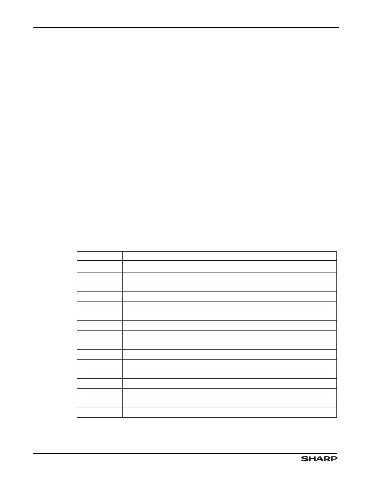
Table 1-3. Port C Settings For Boot
PC[7:4] BOOT CONFIGURATION
0x0 NOR Flash or SRAM; 16-bit data bus; nBLEx is LOW for reads
0x1 NOR Flash or SRAM; 16-bit data bus; nBLEx is HIGH for reads
0x2 NOR Flash or SRAM; 8-bit data bus; nBLEx is LOW for reads
0x3 NOR Flash or SRAM; 8-bit data bus; nBLEx is HIGH for reads
0x4 NAND Flash; 8-bit data bus; 3-byte address
0x5 NAND Flash; 8-bit data bus; 4-byte address
0x6 NAND Flash; 8-bit data bus; 5-byte address
0x7 NAND Flash; 16-bit data bus; 3-byte address
0x8 NOR Flash or SRAM; 32-bit data bus; nBLEx is LOW for reads
0x9 NOR Flash or SRAM; 32-bit data bus; nBLEx is HIGH for reads
0xA Undefined
0xB Undefined
0xC NAND Flash; 16-bit data bus; 4-byte address
0xD NAND Flash; 16-bit data bus; 5-byte address
0xE I
2
C
0xF UART0