I/O Configuration LH79524/LH79525 User’s Guide
11-2 Version 1.0
11.2 Register Reference
This section describes the registers used in I/O configuration. In all cases, when the
MUX register is programmed its corresponding Resistor register (if it exists) must be
programmed. The Resistor registers are not automatically configured.
11.2.1 Memory Map
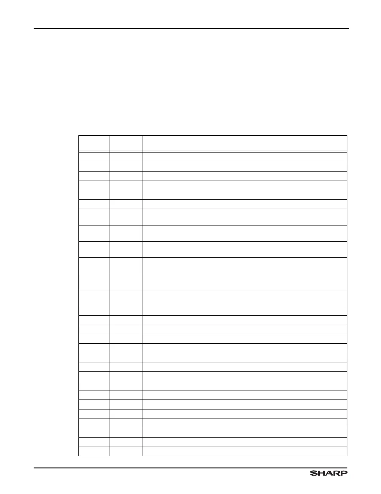
The base address for the IOCON is 0xFFFE5000. Table 11-1 shows the register locations in the
memory map.
Table 11-1. IOCON Register Summary
ADDRESS
OFFSET
NAME DESCRIPTION
0x00 MUXCTL1 Muxing Control 1 For pins from PI2/ETHERCOL to PL0/LCDVD14
0x04 RESCTL1 Resistor Control 1 Assignment for pins From PI2/ETHERCOL to PL0/LCDVD14
0x08 /// Reserved Do not access
0x0C /// Reserved Do not access
0x10 MUXCTL3 Muxing Control 3 For pin INT4/CTCLK/BATCNTL
0x14 RESCTL3 Resistor Control 3 Assignment for pin INT4/CTCLK/BATCNTL
0x18 MUXCTL4
Muxing Control 4 For PA7/CTCAP2B/CTCMP2B/SCL to PA2/CTCAP0A/
CTCMP0A
0x1C RESCTL4
Resistor Control 4 Assignment for pins from PA7/CTCAP2B/CTCMP2B/SCL to
PA2/CTCAP0A/CTCMP0A
0x20 MUXCTL5
Muxing Control 5 For pins from PA1/INT3/UARTTX2/UARTIRTX2 to
PB2/SSPFRM
0x24 RESCTL5
Resistor Control 5 Assignment for pins from PA1/INT3/UARTTX2/UARTIRTX2
to PB2/SSPFRM
0x28 MUXCTL6
Muxing Control 6 For pins from PB1/DREQ/nUARTRTS0 to
PB0/nDACK/nUARTCTS0
0x2C RESCTL6
Resistor Control 6 Assignment for pins from PB1/DREQ/nUARTRTS0 to
PB0/nDACK/nUARTCTS0
0x30 MUXCTL7 Muxing Control 7 For pins from PC7/A23 to PC0/A16
0x34 RESCTL7 Resistor Control 7 Assignment for pins from PC7/A23 to PC0/A16
0x38 /// Reserved Do not access
0x3C /// Reserved Do not access
0x40 /// Reserved Do not access
0x44 /// Reserved Do not access
0x48 MUXCTL10 Muxing Control 10 For pins from PN3/D25 to PK5/D21
0x4C RESCTL10 Resistor Control 10 Assignment for pins from PN3/D25 to PK5/D21
0x50 MUXCTL11 Muxing Control 11 For pins from PD4/D12 to PD1/D9
0x54 RESCTL11 Resistor Control 11 Assignment for pins from PD4/D12 to PD1/D9
0x58 MUXCTL12 Muxing Control 12 For pins from PK0/D16 to PD0/D8
0x5C RESCTL12 Resistor Control 12 Assignment for pins from PK0/D16 to D2
0x60 /// Reserved Do not access
0x64 RESCTL13 Resistor Control 13 Assignment for pins from D1 to D0
0x68 MUXCTL14 Muxing Control 14 For Pins Ranging From nCS3/PM3 to nBLE3/PM5
0x6C /// Reserved Do not access