Watchdog Timer LH79524/LH79525 User’s Guide
19-4 Version 1.0
19.2 Register Reference
This section describes the location and programming of the WDT registers.
19.2.1 Memory Map
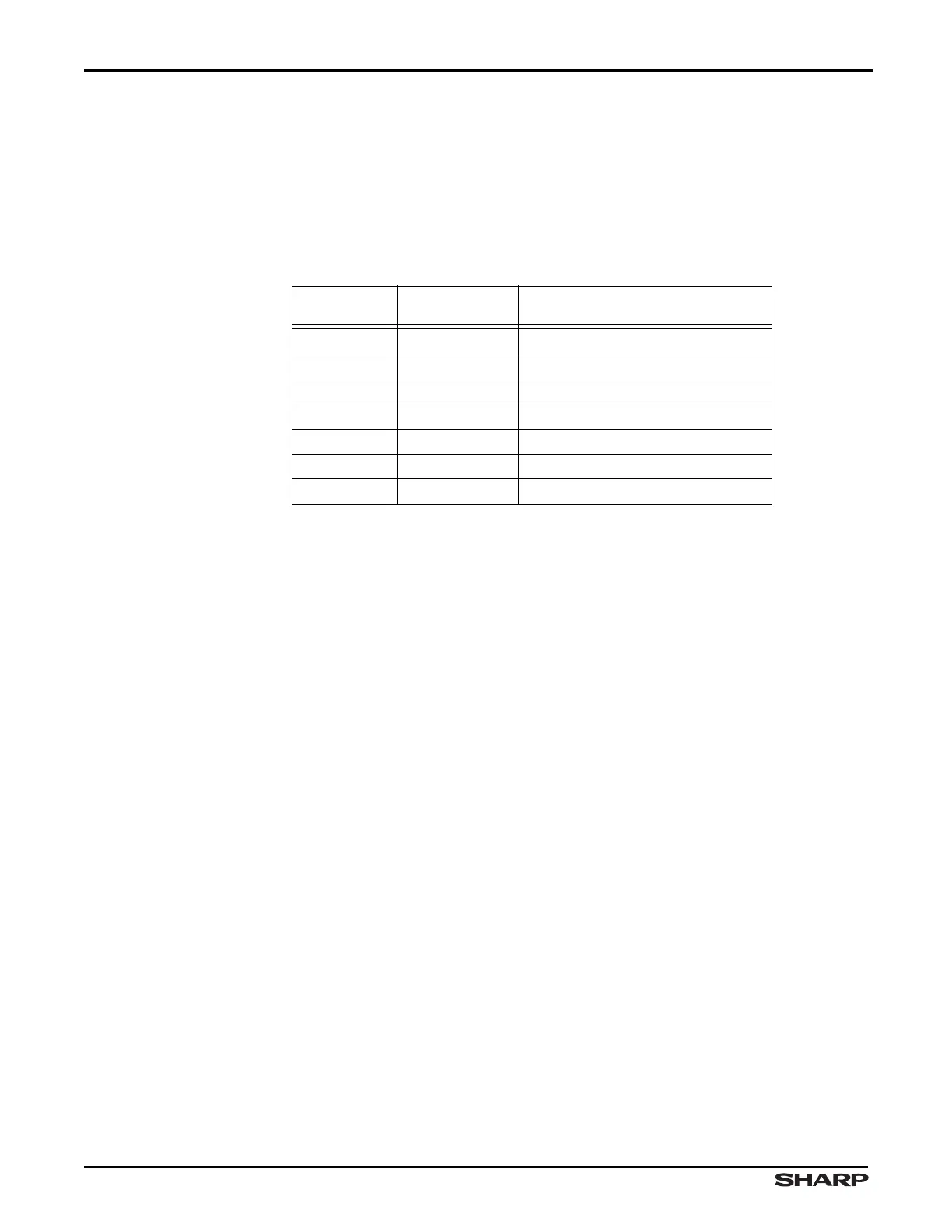
Register offsets in Table 19-1 are relative to the Timer base address 0xFFFC3000.
Table 19-1. Watchdog Timer Memory Map
ADDRESS
OFFSET
NAME DESCRIPTION
0x00 CTL Watchdog Control Register
0x04 RST Watchdog Counter Reset
0x08 STATUS Watchdog Status Register
0x0C COUNT0 Current Count bits [7:0]
0x10 COUNT1 Current Count bits [15:8]
0x14 COUNT2 Current Count bits [23:16]
0x18 COUNT3 Current Count bits [31:24]