Color Liquid Crystal Display Controller LH79524/LH79525 User’s Guide
4-26 Version 1.0
4.5.3.4 Upper Panel Frame Buffer Base Address Register (UPBASE)
The UPBASE Register is one of two Color LCD DMA Base Address Registers (the other
is LPBASE, described in Section 4.5.3.5). Together with LPBASE, this Read/Write regis-
ter programs the base address of the frame buffer.
UPBase is used for:
• TFT displays
• Single-panel STN displays
• The upper panel of dual-panel STN displays.
UPBASE (and LPBASE for dual panels) must be initialized before enabling the CLCDC.
Optionally, the value can be changed mid-frame to allow double-buffered video displays to
be created. These registers are copied to the corresponding current registers at each LCD
vertical synchronization. This event causes the BUI bit and an optional interrupt to be gen-
erated. The BUI bit indicates that it is safe to update both the UPBASE and LPBASE Reg-
isters. The interrupt can be used to reprogram the base address when generating
double-buffered video.
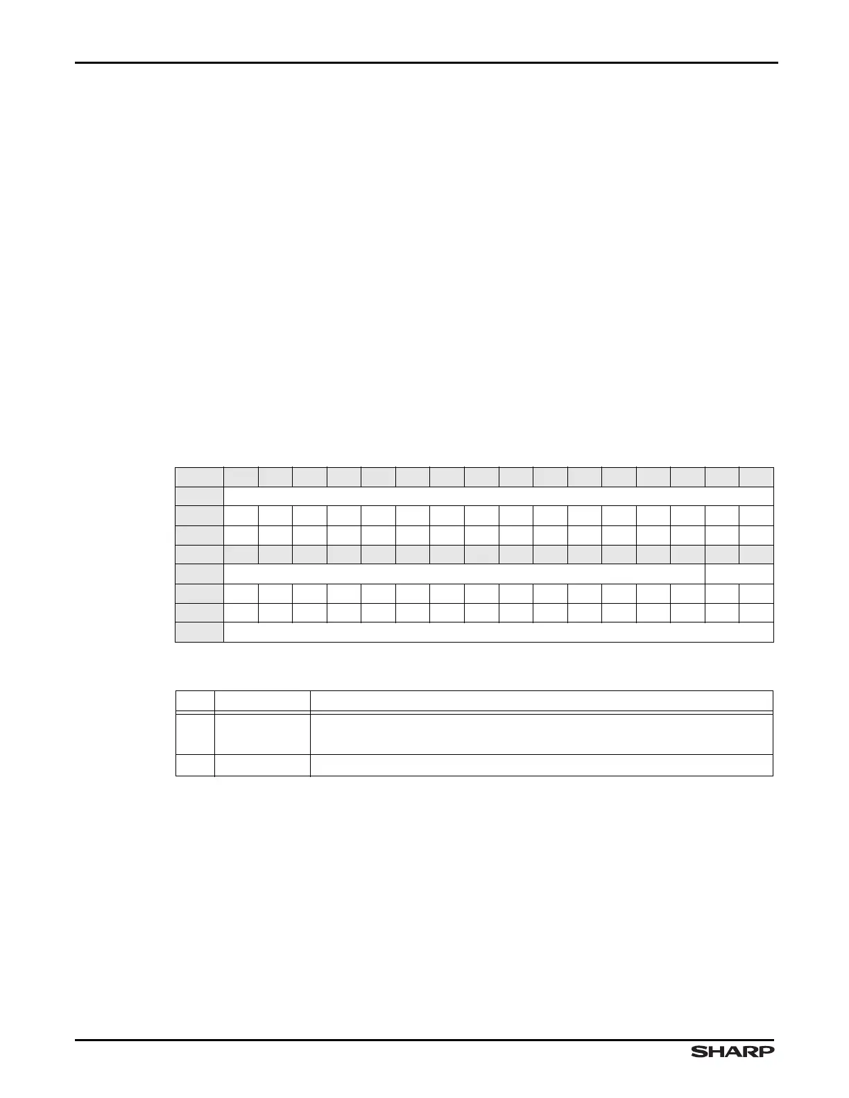
Table 4-20. UPBASE Register
BIT 31 30 29 28 27 26 25 24 23 22 21 20 19 18 17 16
FIELD LCDUPBASE
RESET 0000000000000000
RW RW RW RW RW RW RW RW RW RW RW RW RW RW RW RW RW
BIT 15 14 13 12 11 10 9 8 7 6 5 4 3 2 1 0
FIELD LCDUPBASE ///
RESET 0000000000000000
RW RW RW RW RW RW RW RW RW RW RW RW RW RW RW RO RO
ADDR 0xFFFF4000 + 0x10
Table 4-21. UPBASE Fields
BIT NAME DESCRIPTION
31:2 LCDUPBASE
LCD Upper Panel Base Address This is the start address of the
upper panel frame data stored in memory and is word-aligned.
1:0 /// Reserved Reading returns 0. Write the reset value.