Analog-to-Digital Converter/Brownout Detector LH79524/LH79525 User’s Guide
2-2 Version 1.0
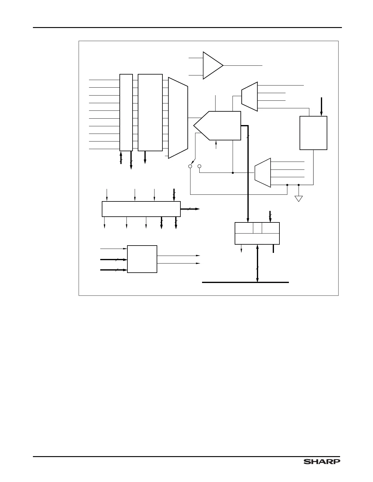
The ADC block can perform a sequence of measurements without intervention from the
ARM core. Examples include:
• Determining touch-screen biasing switch configuration.
• Ascertaining how much settling time is required before making a measurement.
• Determining the ADC input source and ADC reference source.
From 1 to 16 different measurements can be performed in a sequence. The number of
sequence steps is stored in the PC Register.
The biasing switch configuration, settling time, and ADC mux settings for each of the 1 to
16 measurements in the sequence are stored in an entry in the Control Bank. The mea-
surement sequence can be triggered by either software or a Pen Down Interrupt.
Figure 2-1. ADC Block Diagram
LH79525-52
ANALOG
BIAS AND
CONTROL
CLOCK
GENERATOR
CONTROL BANK STATE MACHINE
oscen
CLKSEL
PWM
3
2
11-TO-1
MUX
AN4/WIPER
AN5
AN9
AN8
VREF-
AN3/LR/Y-
AN2/IL/Y+
AN7
AN6/VBAT
AN1/UR/X-
AN0/UL/X+
A2DCLK DIGITAL
EOSINTR
A2DCLK ANALOG
Start_acq A2DON
PWMpenIRQ
EOCA2DCLK DIGITA
HWR
LWR
CBTAG
4-TO-1
MUX
AN8/VREF+EXT
AN0/UL/X+
VLL
GPI
MUX
BrownOut_INTR
VREF
LL/Y+
VREF+
A2DCLK_ANALOG
+REF
+IN
D[9:0]
START
A2D0N
-REF
10b A/D OUT
-IN
4-TO-1
MUX
FIFO
10-BIT
RESULT CBTAGXX
BGAP
VREF
VREF+ EN
VREF-
CBTAG
FwaterINTR FovmINTR
ADVANCED
PERIPHERAL
BUS (APB)
VREF-EXT
AN1/UR/X-
AN3/LR/Y-
VREF-
4
BANDGAPON
4
16
14
2
PenIRQ
15
GPI
GPEN
8
8
10