Synchronous Serial Port LH79524/LH79525 User’s Guide
14-10 Version 1.0
14.2.2 Register Descriptions
14.2.2.1 Control Register 0 (CTRL0)
This register, defined in Table 14-3 and Table 14-4, enables or disables the SSP and con-
trols the serial clock rate, its phase, polarity, data size, and frame format. Bits 3:0 reset to
0b0000 and must be programmed to a valid number prior to using the SSP.
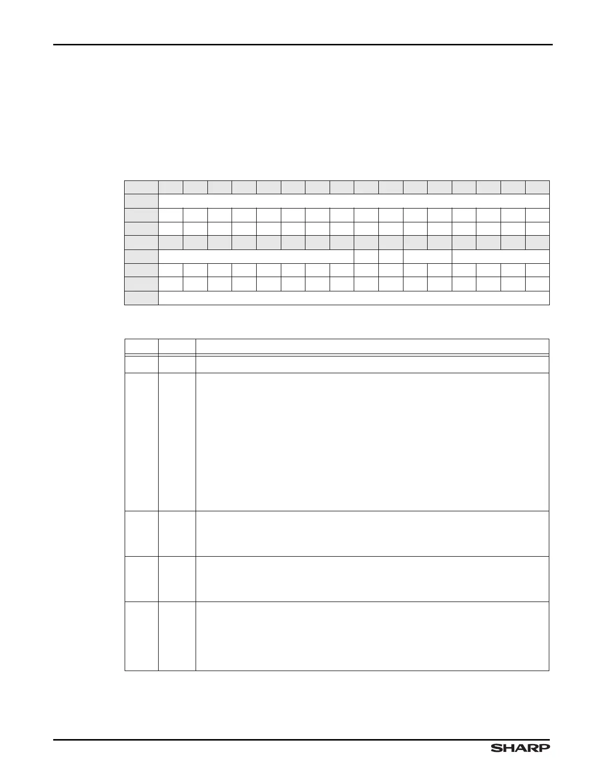
Table 14-3. CTRL0 Register
BIT 31 30 29 28 27 26 25 24 23 22 21 20 19 18 17 16
FIELD ///
RESET 0000000000000000
RW RO RO RO RO RO RO RO RO RO RO RO RO RO RO RO RO
BIT 15 14 13 12 11 10 9 8 7 6 5 4 3 2 1 0
FIELD CPD SPH SPO FRF DSS
RESET 0000000000000000
RW RW RW RW RW RW RW RW RW RW RW RW RW RW RW RW RW
ADDR 0xFFFC6000 + 0x000
Table 14-4. CTRL0 Fields
BITS NAME DESCRIPTION
31:16 /// Reserved Reading returns 0. Write the reset value.
15:8 CPD
Clock Prescale Divisor To generate the bit rate and Serial Clock output
(SSPCLK pin), the SSP uses two divisors on the generated 5.6448 MHz Clock
Input (when using the recommended 11.2896 MHz crystal):
• This programmable clock rate divisor in the CTRL0 register
• A programmable prescaler in the Clock Prescaler register Divisor field
SSPCLK is calculated as follows:
SSPCLK = ƒCLOCK INPUT/(CPSR:DVSR × (1 + CPD))
Program this field to the desired eight-bit CPD value in the above equation. Valid
values are 0 - 0xFF.
7SPH
SSPCLK Phase Applicable to Motorola SPI frame format only.
1 = SSPCLK pin is HIGH when data is not being transferred
0 = SSPCLK pin is LOW when data is not being transferred
6 SPO
SSPCLK Polarity Applicable to Motorola SPI frame format only.
1 = Data is captured on the second clock edge
0 = Data captured on the first clock edge
5:4 FRF
Frame Format Program to select the format for the interface used.
00 = Motorola SPI frame format
01 = TI synchronous serial frame format
10 = National Microwire frame format
11 = Reserved, undefined operation