LH79524/LH79525 User’s Guide General Purpose Input/Output
Version 1.0 8-7
8.2 Register Reference
This section describes the location and programming of the GPIO registers. Registers
are denoted with an ‘x’ that is replaced with the port letter of the register. For example, the
Port A Data Direction Register is P1DDRA.
8.2.1 Memory Map
The base addresses for the GPIO registers are:
Ports A and B: 0xFFFDF000
Ports C and D: 0xFFFDE000
Ports E and F: 0xFFFDD000
Ports G and H: 0xFFFDC000
Ports I and J: 0xFFFDB000
Ports K and L: 0xFFFDA000
Port M and N: 0xFFFD9000
As Port J is an input-only port, the location at base 0xFFFDB000 with an offset of 0x0C
(which would be the space for the Port J Data Direction Register) is reserved. However,
output-only Port M does have a Data Direction Register at location 0xFFFD9000 with an
offset of 0x08, and must be programmed before use.
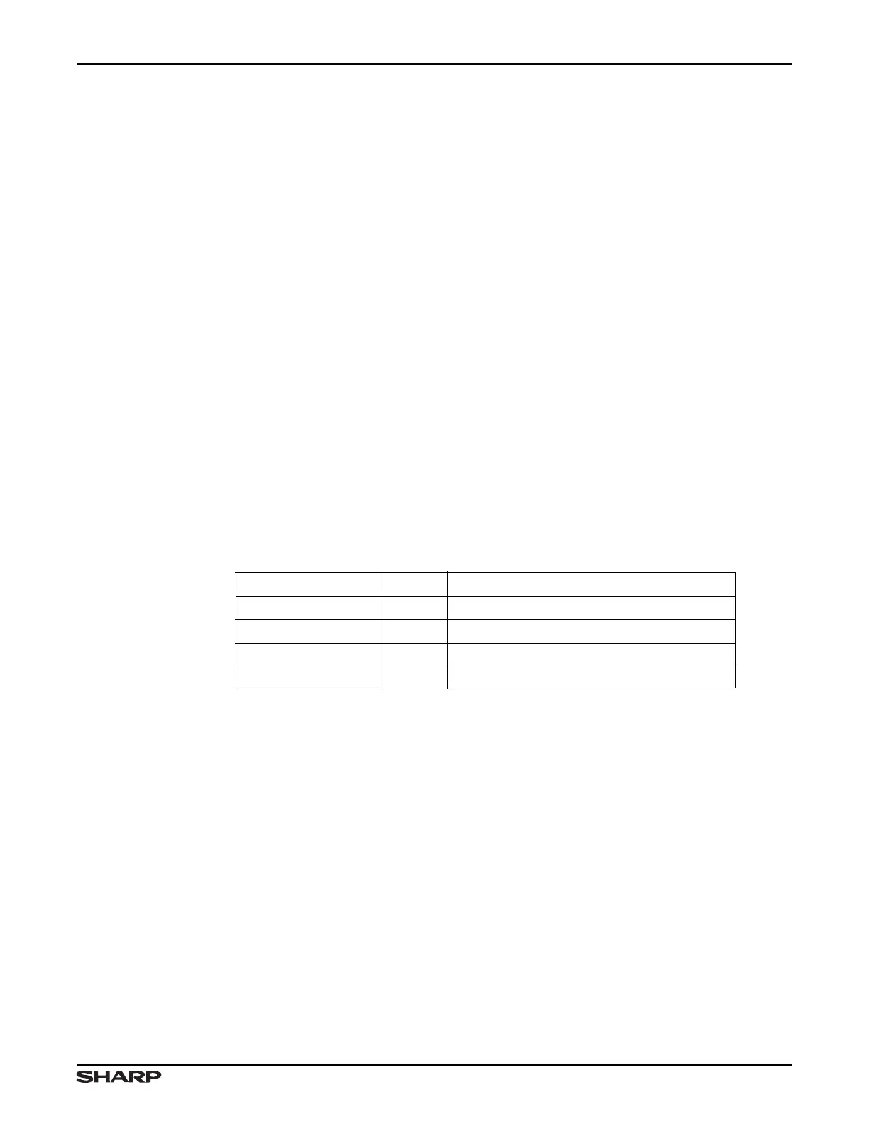
Table 8-4. GPIO Port Memory Map
ADDRESS OFFSET NAME DESCRIPTION
0x00 P1DRx Port A/C/E/G/I/K/M Data Registers
0x04 P2DRx Port B/D/F/H/J/L/N Data Registers
0x08 P1DDRx Port A/C/E/G/I/K/M Data Direction Registers
0x0C P2DDRx Port B/D/F/H/L/N Data Direction Registers