Color Liquid Crystal Display Controller LH79524/LH79525 User’s Guide
4-40 Version 1.0
4.5.6.3 Timing Delay Register 1 (ALITIMING1)
The ALITIMING1 Register is used for various delays values for output signals. All delays
are specified in number of LCD clock (LCDDCLK) periods.
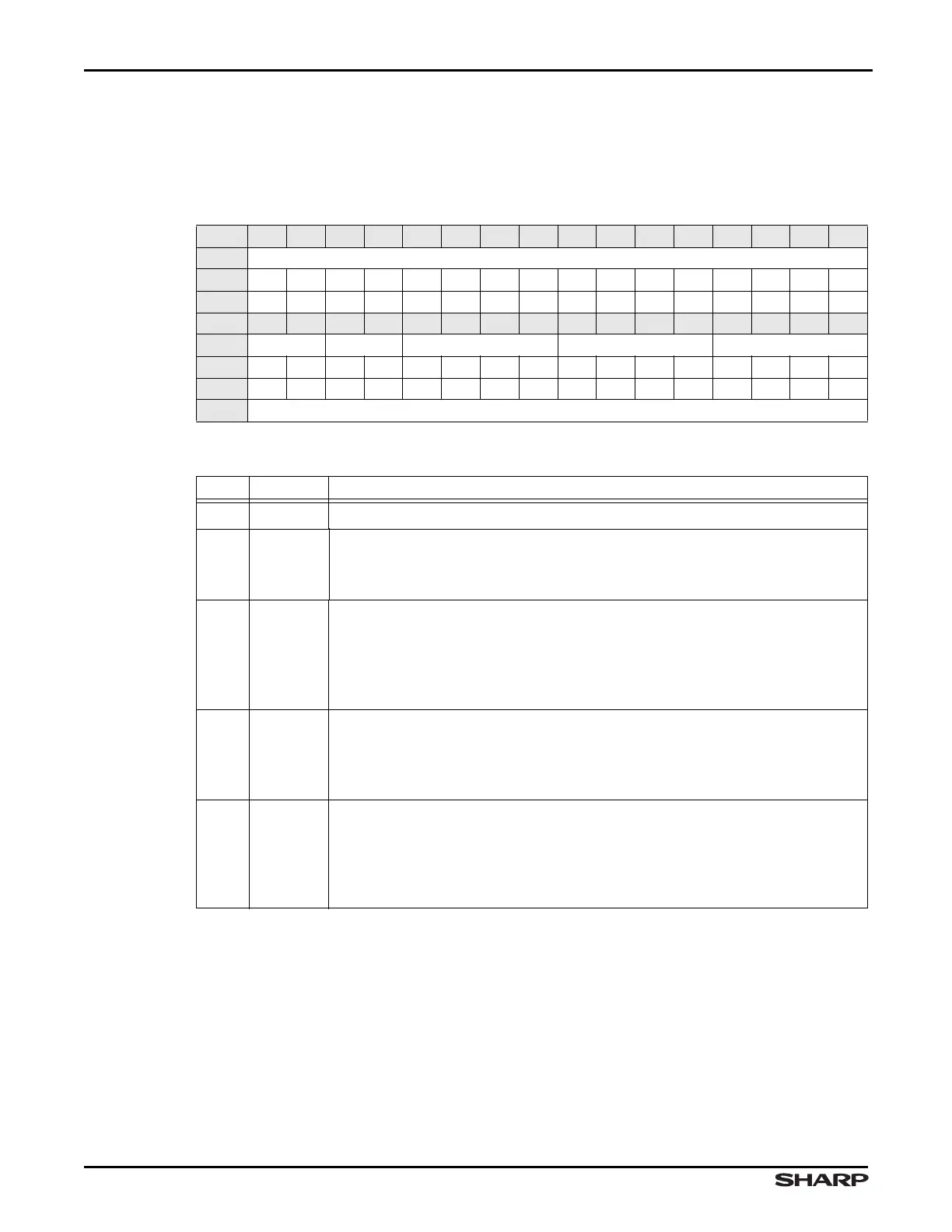
Table 4-47. ALITIMING1 Register
BIT 31 30 29 28 27 26 25 24 23 22 21 20 19 18 17 16
FIELD ///
RESET 0000000000000000
RW RO RO RO RO RO RO RO RO RO RO RO RO RO RO RO RO
BIT 15 14 13 12 11 10 9 8 7 6 5 4 3 2 1 0
FIELD /// MODDEL PSCLS REVDEL LPDEL
RESET 0001000000000000
RW RO RO RW RW RW RW RW RW RW RW RW RW RW RW RW RW
ADDR 0xFFFE4000 + 0x008
Table 4-48. ALITIMING1 Fields
BITS NAME DESCRIPTION
31:14 /// Reserved Reading returns 0. Write the reset value.
13:12 MODDEL
LCDMOD LOW Delay Controls the delay (number of LCDSPS rising edges)
to hold LCDMOD LOW before transitioning HIGH.
MODDEL = (LCDSPS rising edges) – 1
11:8 PSCLS
LCDPS and LCDCLS Delay Controls the delay in LCDDCLK periods from
the first rising edge of the internal CLCDC clock after the leading edge of the
internal LCDLP signal (not the LCDLP pin no. 137), to the leading edge of the
LCDREV signal. The value of this field must be greater than 0.
PSCLS = (LCDDCLK periods) – 1
7:4 REVDEL
Polarity-Reversal Delay* Controls the delay in LCDDCLK periods from the
first assertion of the LCDLP (horizontal sync) signal, to the falling edge of the
LCDREV signal. The value of this field must be greater than 0.
REVDEL = (LCDDCLK periods) – 1
3:0 LPDEL
LCDLP Delay Controls the delay in LCDDCLK periods from the first rising
edge of the internal CLCDC clock after the leading edge of the internal LCDLP
signal (not the LCDLP pin no. 137), to the leading edge of the LCDLP signal.
The value of this field must be greater than 0.
LPDEL = (LCDDCLK periods) – 1