Timers LH79524/LH79525 User’s Guide
15-22 Version 1.0
15.2.2.14 Timer 2 Control Register (CTRL2)
This register allows programming various functions of the timer, including PWM Mode,
clock selection, and start/stop.
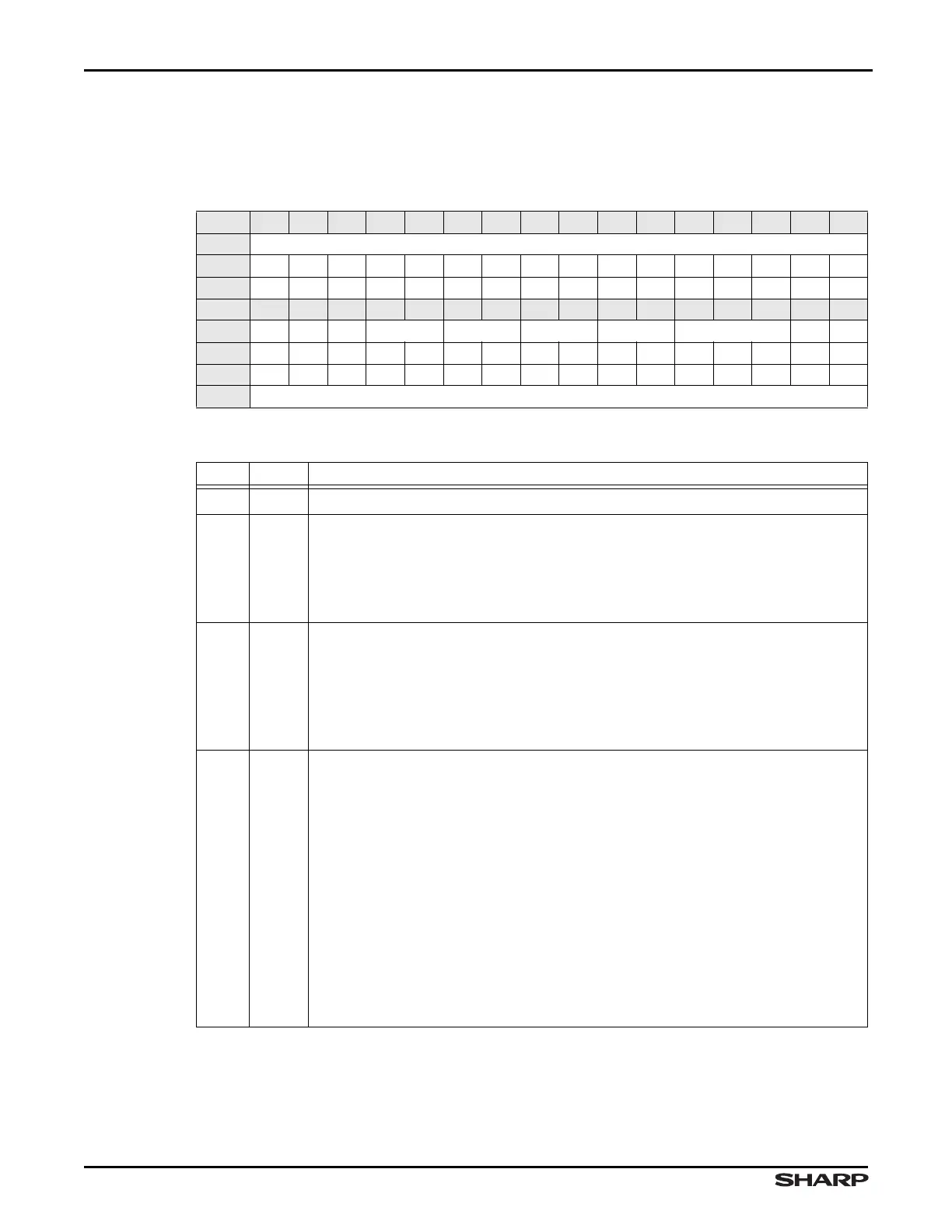
Table 15-30. CTRL2 Register
BIT 31 30 29 28 27 26 25 24 23 22 21 20 19 18 17 16
FIELD ///
RESET 0000000000000000
RW RO RO RO RO RO RO RO RO RO RO RO RO RO RO RO RO
BIT 15 14 13 12 11 10 9 8 7 6 5 4 3 2 1 0
FIELD /// PWM TC CMP1 CMP0 CAPB CAPA SEL CS CCL
RESET 0000000000000000
RW RO RW RW RW RW RW RW RW RW RW RW RW RW RW RW RW
ADDR 0xFFFC4000 + 0x50
Table 15-31. CTRL2 Register Definitions
BITS NAME DESCRIPTION
31:15 /// Reserved Reading this field returns 0. Write the reset value.
14 PWM
PWM Output This bit allows the use of CTCMP2A as a PWM output. This is
done by properly programming this bit as well as other bits in this register. Refer
to Section 15.1.3 for a complete explanation of this feature.
0 = Output CTCMP2A is normal and works only with the CMP2 Register.
1 = Output CTCMP2A is in PWM Mode.
13 TC
Timer 2 Counter Operation This bit determines whether the counter is to oper-
ate as a free running counter or interval counter. When 1, the counter clears upon
matching CMP1 for Timer 2. This operation is only available with the CMP1 Reg-
ister for Timer 2.
0 = Inhibit counter clear (operates as free running counter).
1 = Clear counter when CNT2 for Timer 2 matches CMP1 for Timer 2.
12:11 CMP1
Output Value Select Timer/Counter Operation: Programs the value (when a
compare match occurs) output on the CTCMP2B pin when the CNT2 Register
matches T2CMP1.
00 = No change occurs to CTCMP2B
01 = Output 0 to CTCMP2B
10 = Output 1 to CTCMP2B
11 = Toggle the output to CTCMP2B
PWM Operation:
00 = Invalid
01 = Active HIGH PWM output polarity
10 = Active LOW PWM output polarity
11 = Invalid
IMPORTANT: CMP1 and CMP0 must be programmed to the same polarity.