LH79524/LH79525 User’s Guide Color Liquid Crystal Display Controller
Version 1.0 4-39
4.5.6.2 Control Register (ALICTRL)
ALICTRL is the Control Register. It enables and controls output signals.
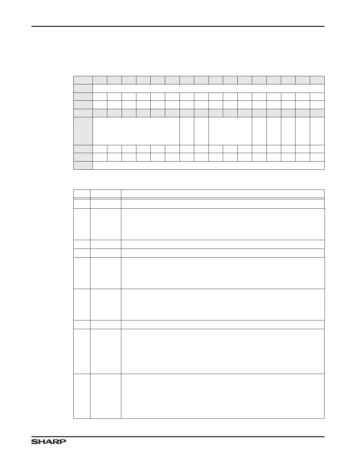
Table 4-45. ALICTRL Register
BIT 31 30 29 28 27 26 25 24 23 22 21 20 19 18 17 16
FIELD ///
RESET 0000000000000000
RW RO RO RO RO RO RO RO RO RO RO RO RO RO RO RO RO
BIT 15 14 13 12 11 10 9 8 7 6 5 4 3 2 1 0
FIELD ///
MODOVRD
MODVAL
///
EN0
DISP
///
CLSEN
SPSEN
RESET 0000000000000000
RW RO RO RO RO RO RO RW RW RO RO RO RW RW RO RW RW
ADDR 0xFFFE4000 + 0x004
Table 4-46. ALICTRL Fields
BITS NAME DESCRIPTION
31:10 ///
Reserved Reading returns 0. Write the reset value.
9 MODOVRD
MOD Signal Override Enable Puts the value of MODVAL directly onto the MOD signal.
0 = LCDMOD pin goes HIGH after the SPS periods specified by the MODDEL field of
the TIMING1 Register.
1 = LCDMOD pin equals the state of MODVAL bit in this register.
8 MODVAL Mod Signal Value Specifies the value to force onto the MOD signal.
7:5 /// Reserved Reading returns 0. Write the reset value.
4EN0
LCDVEEEN Output Enable Specifies the general-purpose output enable to
LCDVEEEN (only in Bypass Mode).
1 = LCDVEEEN signal enabled
0 = LCDVEEEN signal disabled
3DISP
Display Control Signal Output Controls the output of the Display Control signal,
LCDDSPLEN (only in Bypass Mode).
1 = LCDDSPLEN signal enabled
0 = LCDDSPLEN signal disabled
2 /// Reserved Reading returns 0. Write the reset value.
1 CLSEN
CLS Enable
STN or TFT (Bypass) modes: Reserved Reading returns 0. Values written cannot be read.
ALI mode: Enables or disables the generation of the LCDCLS (Gate Driver Clock) signal.
1 = LCDCLS signal enabled
0 = LCDCLS signal disabled
0 SPSEN
SPS Enable
STN or TFT (Bypass) modes: Reserved Reading returns 0. Values written cannot be read.
ALI mode: Enables or disables the generation of the LCDSPS (Row Reset) signal.
1 = LCDSPS signal is enabled
0 = LCDSPS signal is disabled