LH79524/LH79525 User’s Guide Reset, Clock, and Power Controller
Version 1.0 13-23
13.2.2.13 Peripheral Clock Select Register 1 (PCLKSEL1)
This register allows selection of the clock source for the USB, ADC, and SSP peripherals.
Note that the default source for the USB clock following reset is HCLK. For virtually all
designs, this must be programmed to the USB PLL following reset. Failing to do this could
result in the USB Client not operating properly.
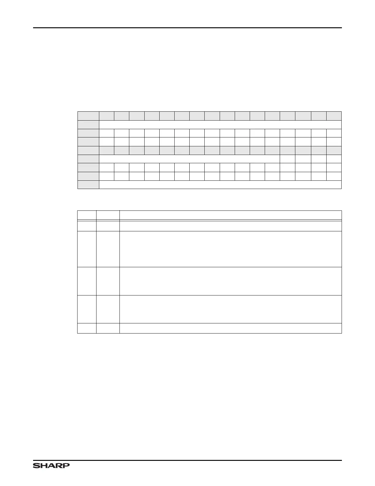
Table 13-30. PCLKSEL1 Register
BIT 31 30 29 28 27 26 25 24 23 22 21 20 19 18 17 16
FIELD ///
RESET 0000000000000000
RW RO RO RO RO RO RO RO RO RO RO RO RO RO RO RO RO
BIT 15 14 13 12 11 10 9 8 7 6 5 4 3 2 1 0
FIELD /// USB ADC SSP ///
RESET 0000000000000000
RW RO RO RO RO RO RO RO RO RO RO RO RO RW RW RW RW
ADDR 0xFFFE2000 + 0x34
Table 13-31. PCLKSEL1 Fields
BITS NAME DESCRIPTION
31:4 /// Reserved Reading returns 0. Write the reset value.
3USB
USB Peripheral Clock Source Following reset, HCLK is the source. In almost
all cases, this should be programmed to 1 following reset.
1 = USB PLL Clock
0 = System Clock (HCLK)
2ADC
ADC Peripheral Clock Source
1 = System Clock Oscillator frequency
0 = System Clock (HCLK)
1 SSP
SSP Peripheral Clock Source
1 = System Clock Oscillator frequency
0 = System Clock (HCLK)
0///Reserved Reading returns 0. Write the reset value.