LH79524/LH79525 User’s Guide Boot Controller
Version 1.0 3-5
3.1.2.2 NAND Flash Hardware Design
The additional NAND Flash control signals are multiplexed with Address lines. Table 3-3
shows the alternate pin functions when using NAND Flash devices.
These alternate pin functions must be considered when designing external interfaces. Fur-
ther, the actual address signals presented on the A22, A23, A3 (ALE), and A4 (CLE) pins
are determined by the memory width being addressed, as described in Section 3.1.2.
The A[4:3] address pins must be written with the correct address to make the ALE and CLE
signals TRUE for the given transaction. These address values differ depending on the
NAND Flash device width being used.
NOTE: Pins A3 and A4 carry different address signals depending on the width of the memory device. For 8-
bit devices, Pin A3= Address signal A3; Pin A4= Address signal A4. For 16-bit devices, Pin A3=
Address signal A4; Pin A4= Address signal A5. For 32-bit devices, Pin A3= Address signal A5; Pin
A4= Address signal A6. See Section 3.1 and Chapter 7: External Memory Controller.
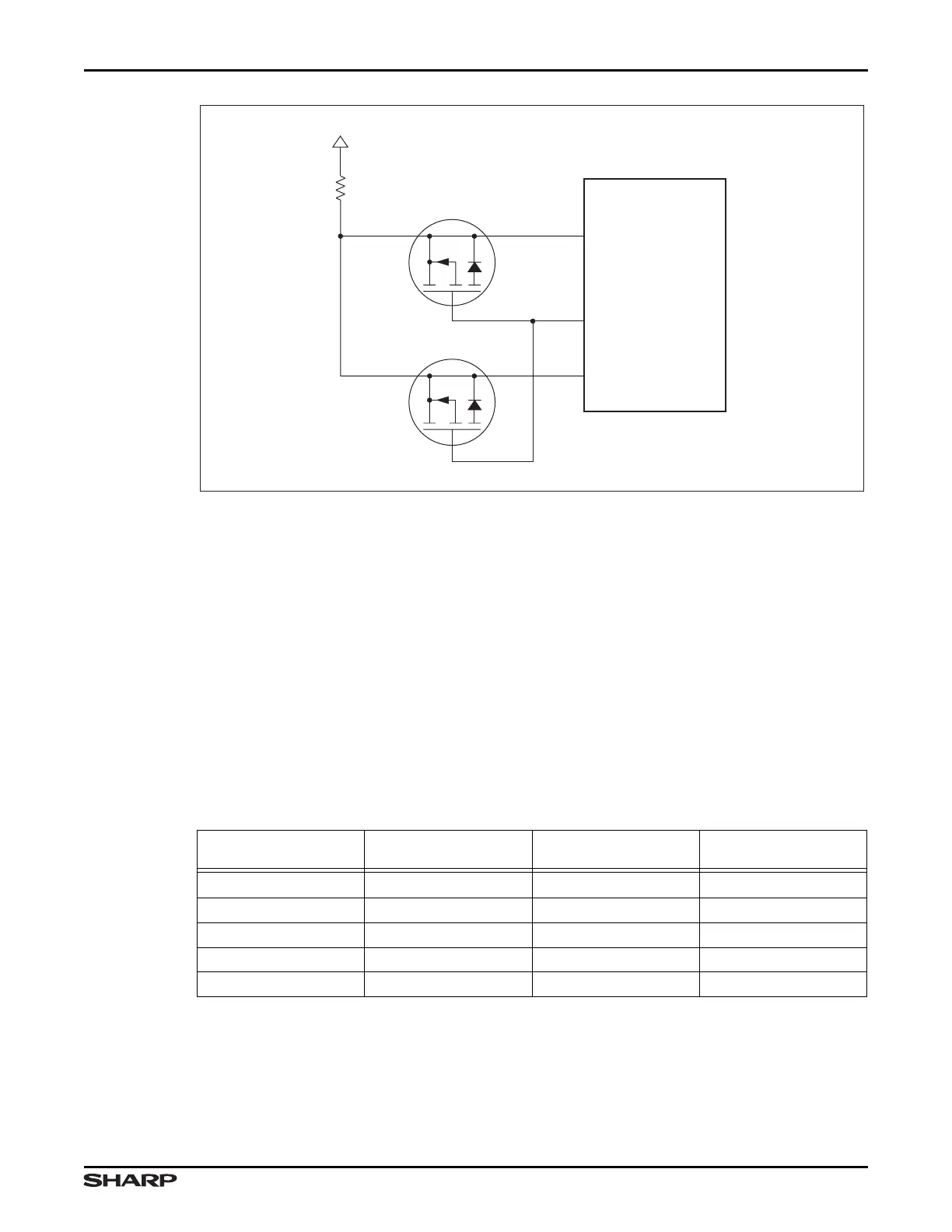
Figure 3-2. Active Pullup Circuit
LH79525-104
LH79524/LH79525
PCy
PCx
nRESETOUT
+3.3 V
120 Ω
1
BSS84
BSS84
32
1
32
Table 3-3. Alternate Pin Function During NAND Flash Booting
PIN
PRIMARY
FUNCTION
SECONDARY
FUNCTION
NAND BOOT
FUNCTION
PC6/A22/nFWE PC6 A22 nFWE
PC7/A23/nFRE PC7 A23 nFRE
A3 A3* N/A ALE
A4 A4* N/A CLE
nCS0 nCS0 N/A nCE