LH79524/LH79525 User’s Guide Analog-to-Digital Converter/Brownout Detector
Version 1.0 2-13
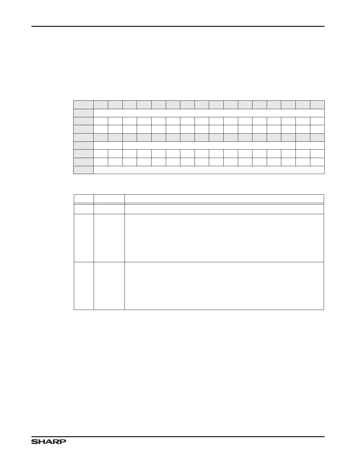
2.2.2.2 Low Word Register (LW)
LW is the Control Bank Low Word Register. This Read Only status register displays the
contents of the current conversion’s low word in the control bank. There is a one-to-one
correspondence between the contents of the control bank low word and the contents of
this register for the current conversion in progress.
Table 2-5. LW Register
BIT 31 30 29 28 27 26 25 24 23 22 21 20 19 18 17 16
FIELD ///
RESET 0000000000000000
RW RO RO RO RO RO RO RO RO RO RO RO RO RO RO RO RO
BIT 15 14 13 12 11 10 9 8 7 6 5 4 3 2 1 0
FIELD /// BIASCON REFM
RESET 0000000000000000
RW RO RO RO RO RO RO RO RO RO RO RO RO RO RO RO RO
ADDR 0xFFFC3000 + 0x04
Table 2-6. LW Fields
BIT NAME DESCRIPTION
31:14
/// Reserved Reading returns 0. Write the reset value.
13:2 BIASCON
Bias Control These bits turn the FETs on and off, as shown in
Figure 2-2. The bit number corresponds to the FET number in the figure.
IMPORTANT: bits 9-11 must always be written as 0b000. Writing a 1 to any
of these three bits can cause unpredictable results.
1 = FET ON
0 = FET OFF
1:0 REFM
Ref- Mux Determines the signal connected to the negative reference of the
ADC during Idle Mode.
00 = VREF- (negative terminal of the internal bandgap reference).
01 = AN1 (UR/X-)
10 = AN3 (LR/Y-)
11 = AN9