Reset, Clock, and Power Controller LH79524/LH79525 User’s Guide
13-20 Version 1.0
13.2.2.10 Peripheral Clock Control Register 1 (PCLKCTRL1)
This register controls the USB, ADC, LCD, and SSP peripheral clocks. Programming a bit
to 1 disables the corresponding peripheral’s clock. The SSP Clock, USB Clock, and the
LCD Data Clock are more fully described in Table 13-1. The ADC Clock is described in
Section 2.1.3 of this User’s Guide.
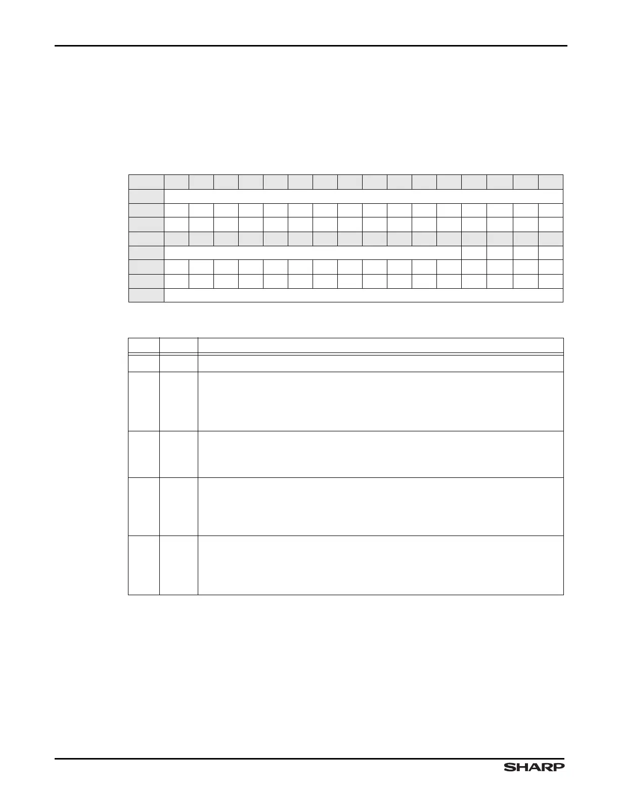
Table 13-24. PCLKCTRL1 Register
BIT 31 30 29 28 27 26 25 24 23 22 21 20 19 18 17 16
FIELD ///
RESET 0000000000000000
RW RO RO RO RO RO RO RO RO RO RO RO RO RO RO RO RO
BIT 15 14 13 12 11 10 9 8 7 6 5 4 3 2 1 0
FIELD /// USB ADC SSP LCD
RESET 0000000000001111
RW RO RO RO RO RO RO RO RO RO RO RO RO RW RW RW RW
ADDR 0xFFFE2000 + 0x28
Table 13-25. PCLKCTRL1 Fields
BITS NAME DESCRIPTION
31:4 /// Reserved Reading returns 0. Write the reset value.
3USB
USB Clock Enables and disables the internal 48 MHz clock to the USB Device
peripheral.
1 = Stops the USB Clock
0 = Enables the USB Clock
2ADC
ADC Clock Enables and disables the internal ADC clock generator.
1 = Stops the ADC Clock
0 = Enables the ADC Clock
1 SSP
SSP Clock (SSPCLK) Enables and disables the clock presented to the
SSPCLK pin.
1 = Stops the SSP Clock
0 = Enables the SSP Clock.
0LCD
LCD Data Clock (LCDDCLK) Enables and disables the clock presented to the
Color LCD Contoller hardware and the LCDDCLK pin.
1 = Stops the LCD Data Clock
0 = Enables the LCD Data Clock