LH79524/LH79525 User’s Guide Synchronous Serial Port
Version 1.0 14-15
14.2.2.5 Clock Prescale Register (CPSR)
The CPSR Register specifies the division factor by which the input HCLK is internally
divided before use. The value programmed into this register is a value from 2 to 254. This
register defaults to zero, but is double buffered and reads back 1s after Reset.
Because
it resets to zero, it must be programmed prior to enabling the SSP.
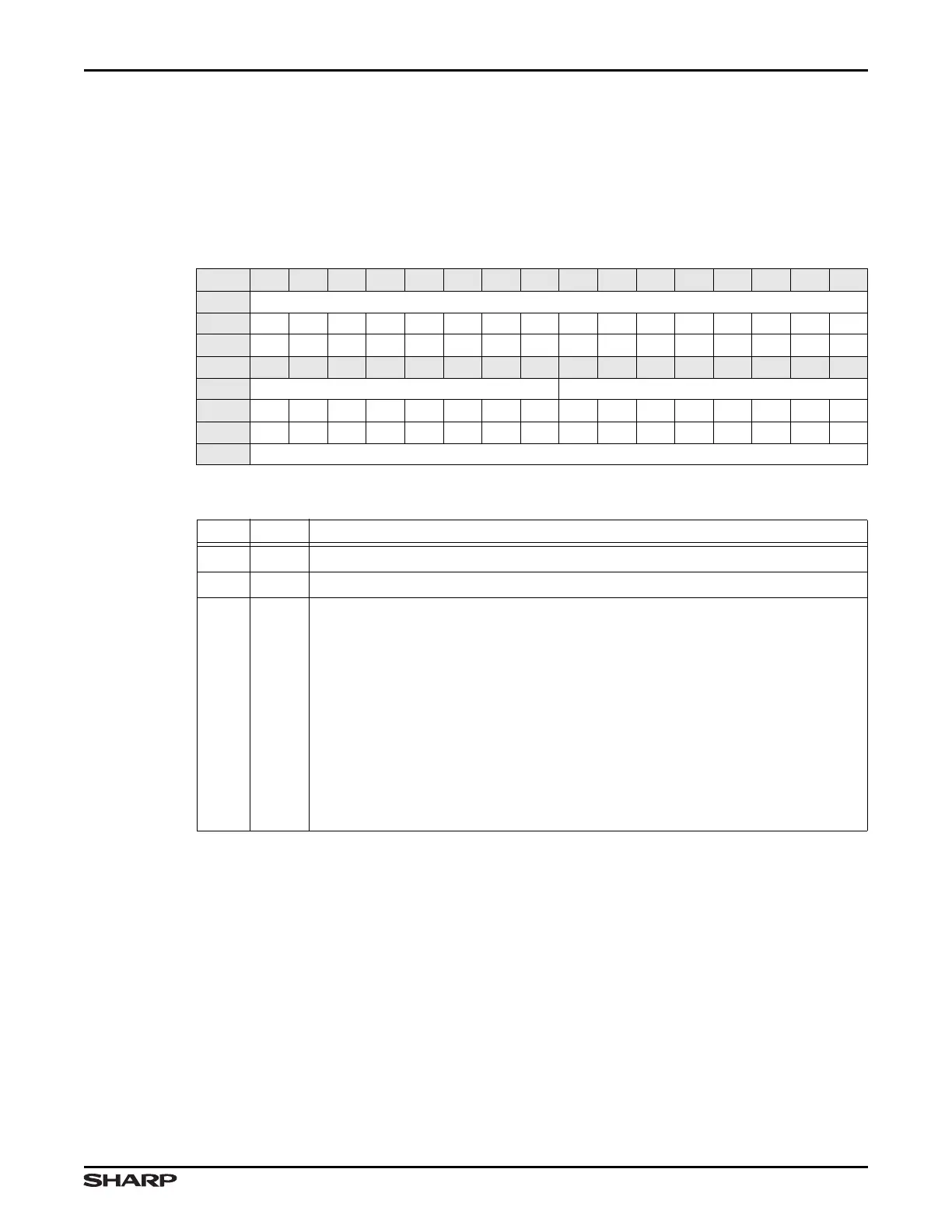
Table 14-11. CPSR Register
BIT 31 30 29 28 27 26 25 24 23 22 21 20 19 18 17 16
FIELD ///
RESET 0000000000000000
RW RO RO RO RO RO RO RO RO RO RO RO RO RO RO RO RO
BIT 15 14 13 12 11 10 9 8 7 6 5 4 3 2 1 0
FIELD /// DVSR
RESET 0000000000000000
RW WO WO WO WO WO WO WO WO RW RW RW RW RW RW RW RO
ADDR 0xFFFC6000 + 0x010
Table 14-12. CPSR Fields
BITS NAME DESCRIPTION
31:16 /// Reserved Reading returns 0. Write the reset value.
15:8 /// Reserved Write as zero. Unpredictable behavior when read.
7:0 DVSR
Clock Prescale Divisor To generate the bit rate and Serial Clock output
(SSPCLK), the SSP uses two divisors on the generated 5.6448 MHz Clock
Input (when using the recommended 11.2896 MHz crystal):
• This programmable prescaler in the Clock Prescaler register Divisor field
• A programmable clock rate divisor in the CTRL0 register (CTRL0:CPD)
Program this field to the desired even-number eight-bit value between 2 and 254 for
DVSR shown in the equation (note that bit zero is always 0, hence DVSR is always
an even number).
SSPCLK is calculated as follows:
SSPCLK = ƒCLOCK INPUT/(DVSR × (1 + CPD))