Reset, Clock, and Power Controller LH79524/LH79525 User’s Guide
13-8 Version 1.0
13.2 Register Reference
This section provides the RCPC register memory mapping and bit fields.
13.2.1 Memory Map
The base address for the RCPC is: 0xFFFE2000.
13.2.2 Register Descriptions
Except where noted, all registers are both writable and readable. Unless noted, unpredict-
able behavior results from writing anything but the reset values to any reserved location.
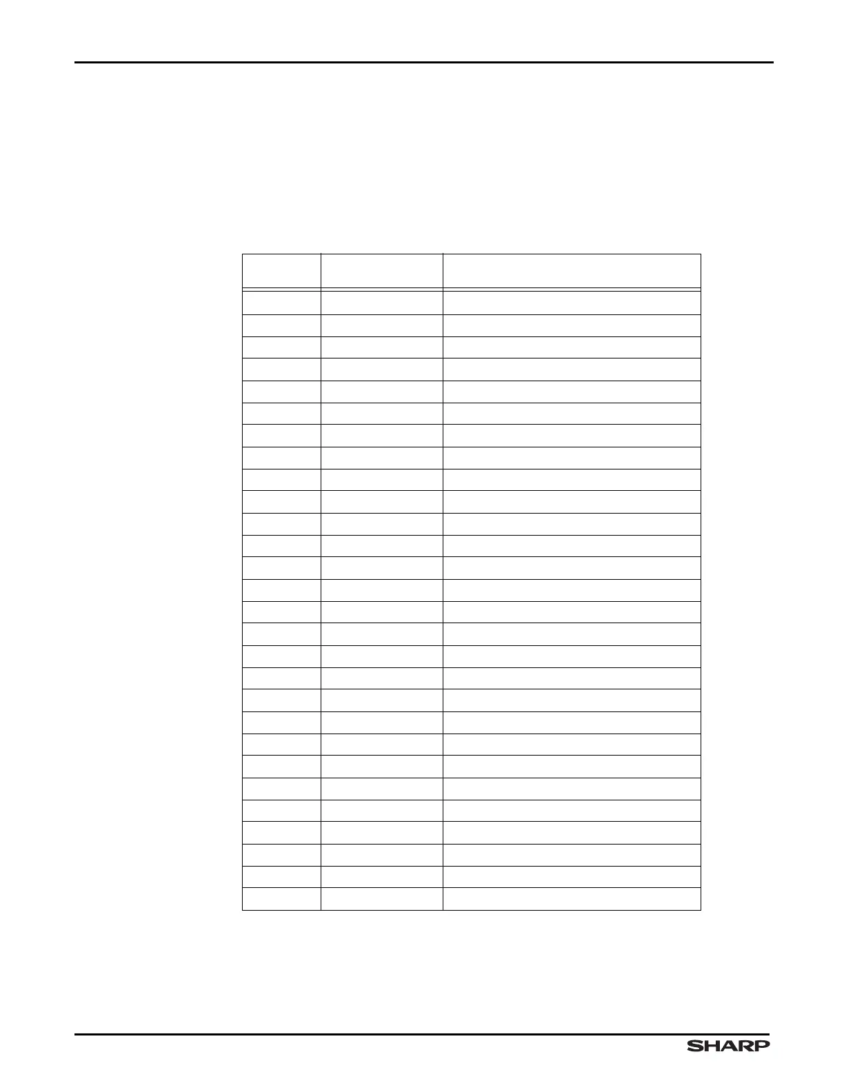
Table 13-3. RCPC Register Summary
ADDRESS
OFFSET
NAME DESCRIPTION
0x00 CTRL RCPC Control Register
0x04 CHIPID Chip Identification Register
0x08 REMAP Remap Control Register
0x0C SOFTRESET Soft Reset Register
0x10 RSTSTATUS Reset Status Register
0x14 RSTSTATUSCLR Reset Status Clear Register
0x18 SYSCLKPRE System Clock Prescaler Register
0x1C CPUCLKPRE CPU Clock Prescaler Register
0x20 /// Reserved — Do not access
0x24 PCLKCTRL0 Peripheral Clock Control 0 Register
0x28 PCLKCTRL1 Peripheral Clock Control 1 Register
0x2C AHBCLKCTRL AHB Clock Control
0x30 PCLKSEL0 Peripheral Clock Select Register 0
0x34 PCLKSEL1 Peripheral Clock Select Register 1
0x38 /// Reserved — Do not access
0x3C SILICONREV Silicon Revision Register
0x40 LCDPRE LCD Prescaler Register
0x44 SSPPRE SSP Prescaler Register
0x48 ADCPRE ADC Prescaler Register
0x4C USBPRE USB Prescaler Register
0x50-0x7C /// Reserved — Do not access
0x80 INTCONFIG External Interrupt Configuration Register
0x84 INTCLR External Interrupt Clear Register
0x88 CORECONFIG Core Clock Configuration Register
0x8C /// Reserved — Do not access
0xC0 SYSPLLCNTL System PLL Control Register
0xC4 USBPLLCTL USB PLL Control Register
0xC8 /// Reserved — Do not access