Version 1.0 1-1
Chapter 1
Overview
The LH79524 and LH79525 are fully-integrated 16/32-bit Systems-on-Chip (SoCs) based
on a 32-bit ARM720T core. The 32-bit ARM720T RISC core provides a powerful instruc-
tion set and includes Cache RAM, a Write Buffer, Memory-Management Unit (MMU), and
Translation Lookaside Buffer (TLB). Both SoCs include a Color LCD Controller, a Direct
Memory Access Controller, Vectored Interrupt Controller, 16KB of internal Static RAM
(SRAM), and several supporting peripherals. The External Memory Controller (EMC),
provides a glueless interface to external memory.
Supporting function blocks within the LH79524/LH79525 include Serial and Parallel Inter-
faces, Counters/Timers, Real Time Clock, Watchdog Timer, Pulse Width Modulators, and
an on-chip Phase-Locked Loop. JTAG support is provided to simplify debugging.
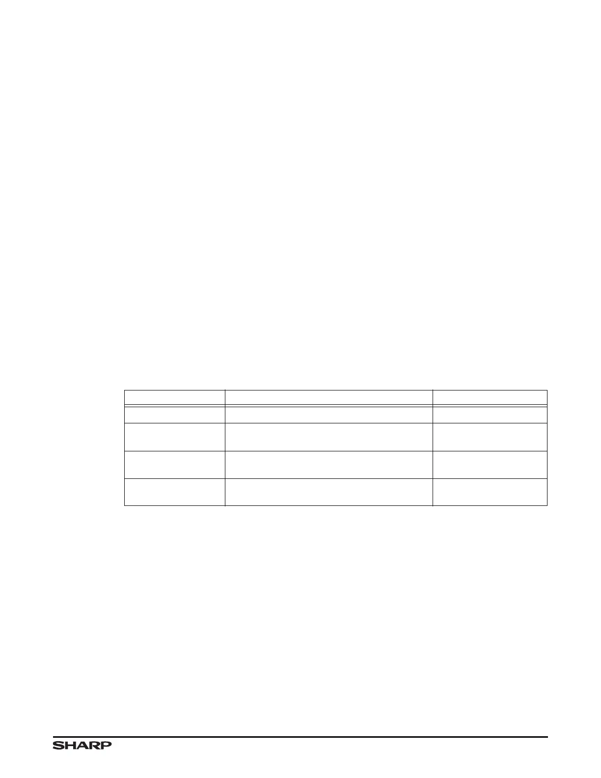
Table 1-1 summarizes the differences in features between the LH79524 and the LH79525.
All other peripherals and functional blocks are identical (unless noted in the Chapter detail-
ing that block’s function). The block diagram for both devices appears in Figure 1-1. Refer
to it when reading sections detailing bus architecture and functional block descriptions.
Table 1-1. LH79524/LH79525 Differences
FEATURE LH79524 LH79525
Package 208 CABGA 176 LQFP
Data Bus Width
32-Bit Data Bus that includes
all peripherals
16-bit Data Bus that
includes all peripherals
Color LCD Controller
(CLCDC)
16-bit CLCDC Data 12-bit CLCDC Data
General Purpose
Input/Output (GPIO)
92 GPIO, 8 General Purpose Input only (GPI),
8 General Purpose Output only (GPO)
72 GPIO, 8 GPI, 6 GPO