LH79524/LH79525 User’s Guide Universal Serial Bus Device
Version 1.0 17-33
17.2.3.14 DMA Channel x Control Register (CNTLx)
This register allows configuring various functions for DMA Channels 1 through 6.
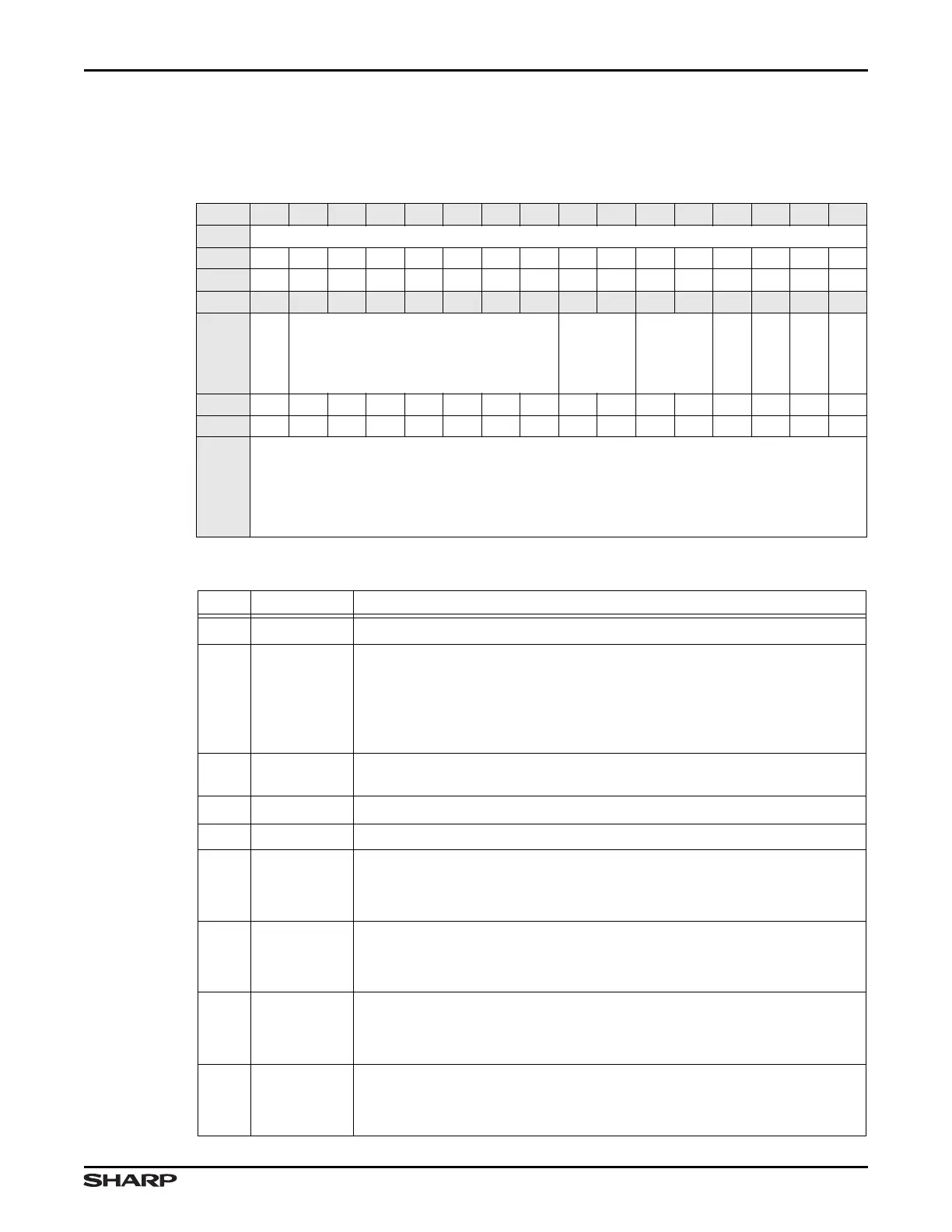
Table 17-50. CNTLx Register
BIT 31 30 29 28 27 26 25 24 23 22 21 20 19 18 17 16
FIELD ///
RESET 0000000000000000
TYPE RO RO RO RO RO RO RO RO RO RO RO RO RO RO RO RO
BIT 15 14 13 12 11 10 9 8 7 6 5 4 3 2 1 0
FIELD
BUS_ERR
MAX /// ENDPOINT
INTEN
MODE
DIRECTION
EN
RESET 0000000000000000
TYPE RW RW RW RW RW RW RW RW RO RO RW RW RW RW RW RW
ADDR
Channel 1 = 0xFFFF5000 + 0x204
Channel 2 = 0xFFFF5000 + 0x214
Channel 3 = 0xFFFF5000 + 0x224
Channel 4 = 0xFFFF5000 + 0x234
Channel 5 = 0xFFFF5000 + 0x244
Channel 6 = 0xFFFF5000 + 0x254
Table 17-51. CNTLx Fields
BITS NAME FUNCTION
31:16
/// Reserved Reading returns 0. Write the reset value.
15 BUS_ERR
Bus Error If a bus error occurs while DMA is accessing memory on the
AHB, the DMA controller immediately terminates the DMA transfer and
interrupts the processor by setting this bit.
1 = Bus error occurred
0 = No bus error
14:8 MAX
Max Packet Size Program with the maximum packet size, in units of 8
bytes (required for Mode 1 only).
7:6
/// Reserved Reading returns 0. Write the reset value.
5:4 ENDPOINT Endpoint Number Program the endpoint number into this field (0-3).
3INTEN
Interrupt Enable
1 = Enable interrupt
0 = Disable interrupt
2DMA_MODE
DMA Operation Mode See full description in Table 17-39.
1 = DMA Mode 1
0 = DMA Mode 0
1 DIRECTION
Data Direction
1 = IN endpoint
0 = OUT endpoint
0DMAEN
DMA Enable
1 = Enable DMA
0 = Disable DMA