LH79524/LH79525 User’s Guide Color Liquid Crystal Display Controller
Version 1.0 4-15
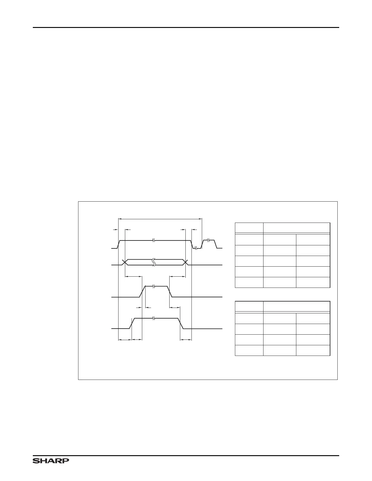
4.3.9 LCD Power Sequencing at Turn-On and Turn-Off
Many LCD panels require ground, power for the digital logic, and high-voltage power sup-
plies. To extend the life of these panels, the digital power must be applied before the high
voltage is applied, and removed after they are removed. The logic signals driving the panel
must be active before the panel voltages are applied, and the panel voltages must be
removed before the logic signals are removed. This sequencing ensures that the panel is
always operated with a net DC bias of 0 VDC.
Software must ensure that these conditions are met. The requisite delay is usually speci-
fied in the LCD panel’s data sheet. If the proper power sequencing is not followed, the LSI
drivers in the panel can latch and the display will freeze. Typically when this happens, the
colors will be incorrect on STN panels. In addition the power down sequence must be fol-
lowed or LCD life can be degraded.
Figure 4-4 is an example of these timing requirements for the SHARP LM057QCTT03
Color STN LCD Panel, and the accompanying timing specifications. Always refer to your
specific LCD panel’s Data Sheet to determine the specific turn-on and turn-off require-
ments for the panel being used in your application.
Figure 4-4. LCD Panel Power Sequencing
Note
tVLD
VDD
DISP
VEE
YD, LP,
XCK, DATA
tDC
tCR
tVLVP tVPD
NOTE: 500 ms MIN. ON/OFF cycle time. All signals and power must be
switched in this sequence during power ON/OFF cycles.
tRCVP
tRVPVL
tRCD
tRDVL
POWER ON
SYMBOL
tVLD
tDC
tCR
tVPD
tVLVP
0 ms MIN. 1 sec. MAX.
100 ns MAX.
20 ms MIN.
0 ms MIN.
0 ms MIN.
ALLOWABLE VALUE
POWER OFF
SYMBOL
tRDVL
tRCD
tRCVP
tRVPVL
0 ms MIN. 1 sec. MAX.
20 ms MIN.
0 ms MIN.
20 ms MIN.
ALLOWABLE VALUE
79525-47