LH79524/LH79525 User’s Guide Synchronous Serial Port
Version 1.0 14-9
14.2 Register Reference
This section provides the SSP’s register memory mapping and bit fields.
14.2.1 Memory Map
The base address for the SSP is 0xFFFC6000. Locations at offsets 0x028 through 0xFFF
are reserved and must not be accessed.
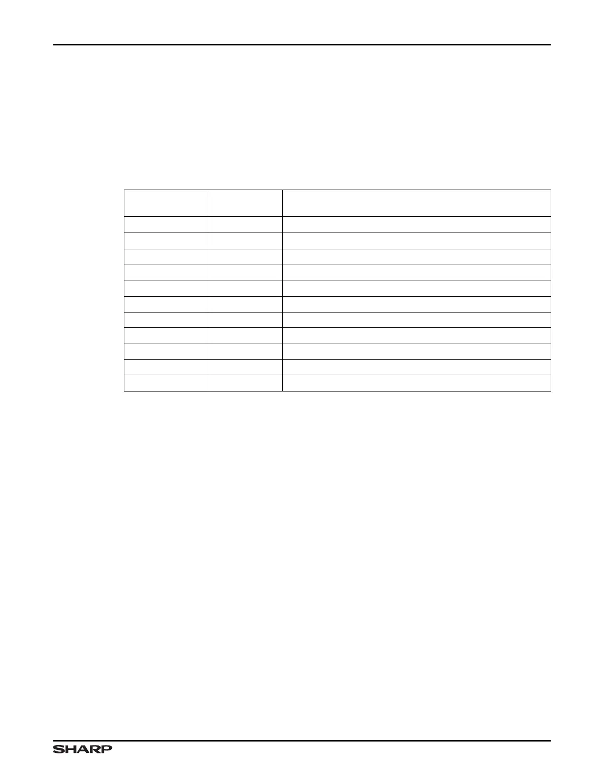
Table 14-2. SSP Register Summary
ADDRESS
OFFSET
NAME DESCRIPTION
0x000 CTRL0 Control Register 0
0x004 CTRL1 Control Register 1
0x008 DR Data Register
0x00C SR Status Register
0x010 CPSR Clock Prescale Register
0x014 IMSC Interrupt Mask Set and Clear Register
0x018 RIS Raw Interrupt Status Register
0x01C MIS Masked Interrupt Status Register
0x020 ICR Interrupt Clear Register
0x024 DCR DMA Control Register
0x028 - 0xFFF /// Reserved — Do not access