Analog-to-Digital Converter/Brownout Detector LH79524/LH79525 User’s Guide
2-10 Version 1.0
2.2 Register Reference
This section provides the ADC and Brownout Detector register memory mapping and
bit fields.
2.2.1 Memory Map
The base address for the ADC is 0xFFFC3000.
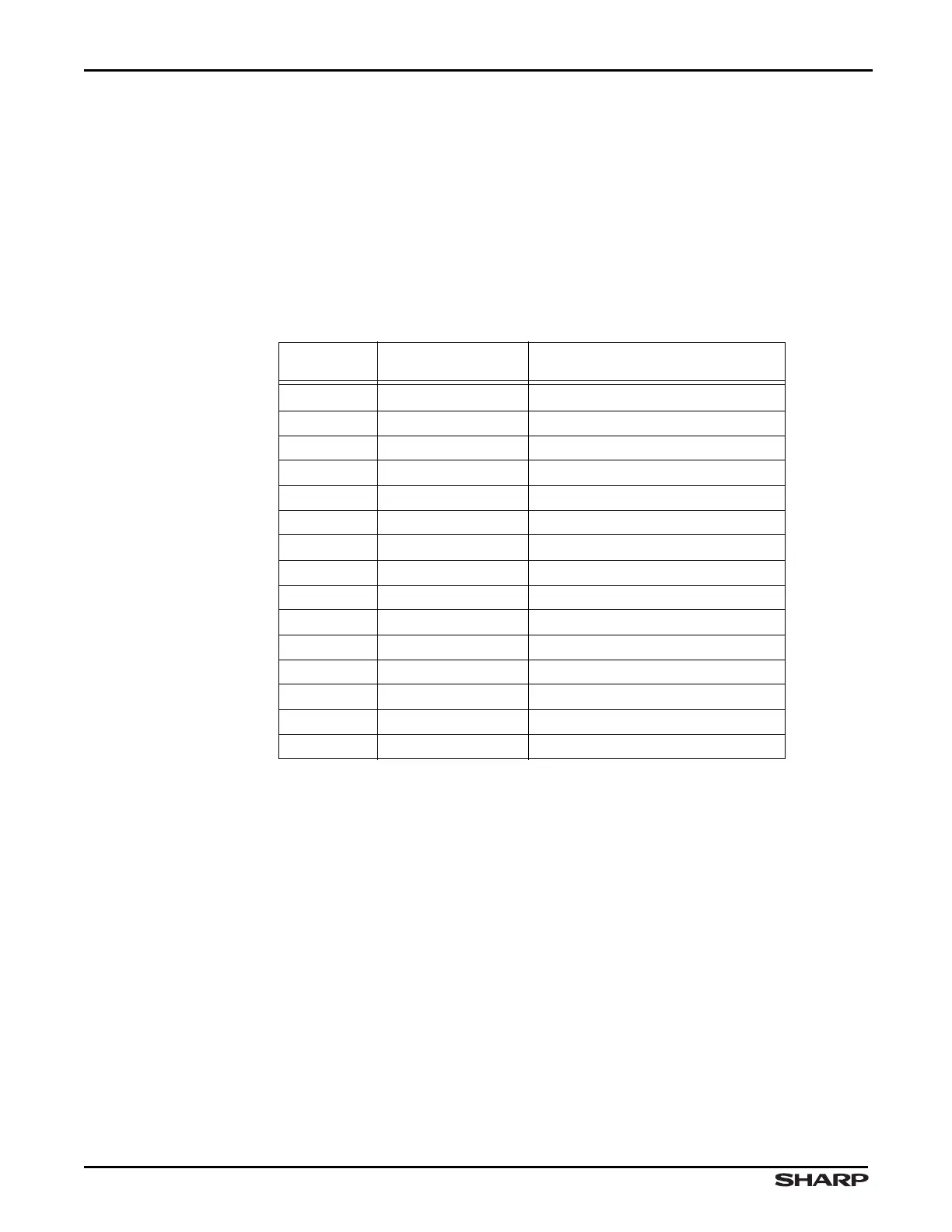
Table 2-1 Summarizes the ADC registers. Address offsets in the table are from the base
address. All registers are little endian format.
Table 2-1. ADC Register Summary
ADDRESS
OFFSET
NAME DESCRIPTION
0x00 HW High Word Register
0x04 LW Low Word Register
0x08 RR Results Register
0x0C IM Interrupt Masking Register
0x10 PC Power Configuration Register
0x14 GC General Configuration Register
0x18 GS General Status Register
0x1C IS Interrupt Status Register
0x20 FS FIFO Status Register
0x24 - 0x60 HWCB0 - HWCB15 High Word Control Bank Registers
0x64 - 0xA0 LWCB0 - LWCB15 Low Word Control Bank Registers
0xA4 IHWCTRL Idle High Word Registers
0xA8 ILWCTRL Idle Low Word Registers
0xAC MIS Masked Interrupt Status
0xB0 IC Interrupt Clear Register