General Purpose Input/Output LH79524/LH79525 User’s Guide
8-8 Version 1.0
8.2.2 Register Descriptions
8.2.2.1 Port A/C/E/G/I/K/M Data Registers (P1DRx)
Values written to P1DRx are output on the PA/PC/PE/PG/PI/PK/PM pins if the correspond-
ing P1DDRx Data Direction bits are set for output. When the corresponding Data Direction
Register bit for a pin is set for input, the value read is the state of the GPIO pin. Reading
this register returns either:
• The last bit value written if the bit is configured as an output.
• The current value on the corresponding port pin if configured as an input.
Port K is only available on the LH79524. Port M is an output only port. This register will not
input values from the Port M pins.
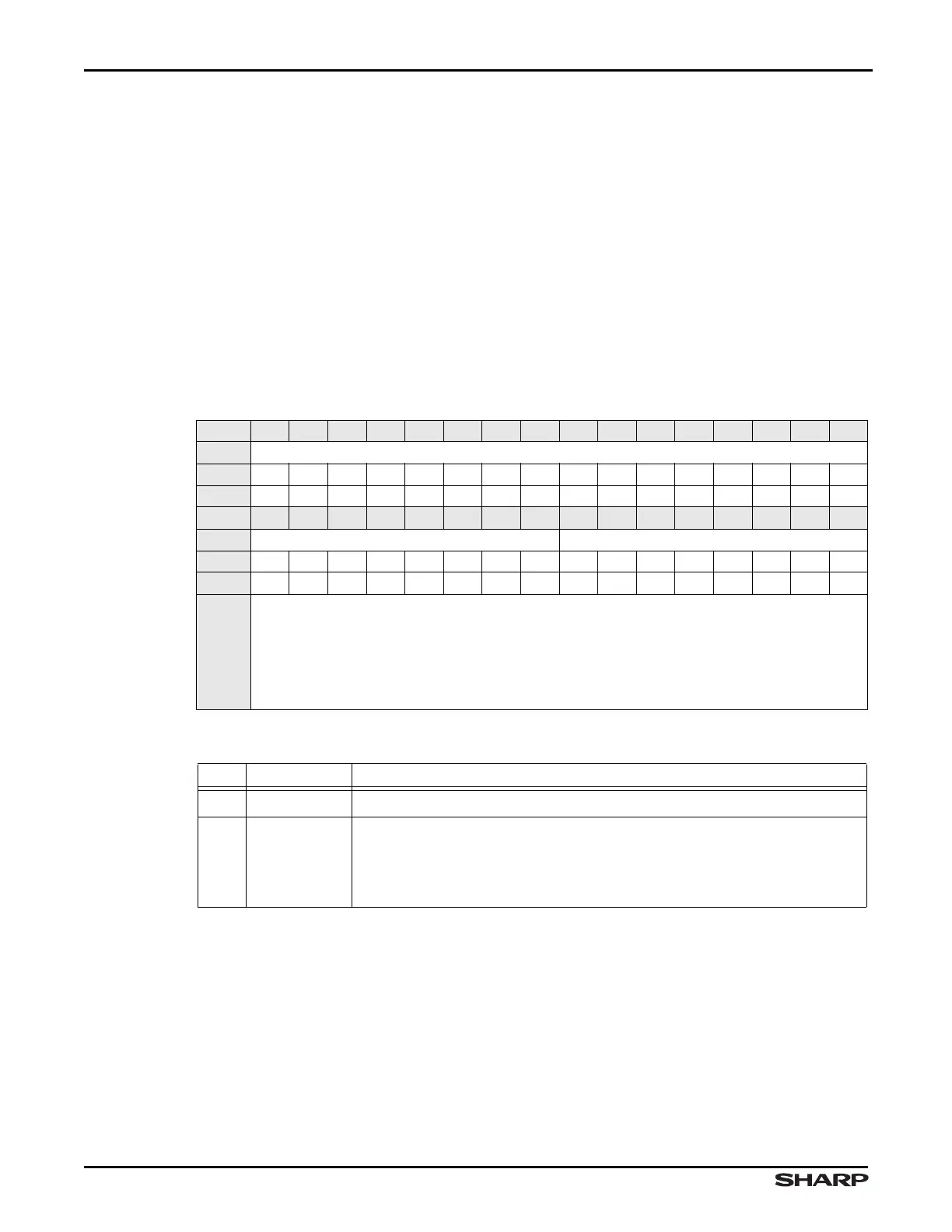
Table 8-5. P1DRx Register
BIT 31 30 29 28 27 26 25 24 23 22 21 20 19 18 17 16
FIELD ///
RESET 0000000000000000
RW RO RO RO RO RO RO RO RO RO RO RO RO RO RO RO RO
BIT 15 14 13 12 11 10 9 8 7 6 5 4 3 2 1 0
FIELD /// PORT_DATA
RESET 0000000000000000
RW RO RO RO RO RO RO RO RO RW RW RW RW RW RW RW RW
ADDR
Port A: 0xFFFDF000 + 0x00
Port C: 0xFFFDE000 + 0x00
Port E: 0xFFFDD000 + 0x00
Port G: 0xFFFDC000 + 0x00
Port I: 0xFFFDB000 + 0x00
Port K: 0xFFFDA000 + 0x00 (LH79524 Only)
Port M: 0xFFFD9000 + 0x00 (Bits 7 and 6 LH79524 Only)
Table 8-6. P1DRx Fields
BITS NAME DESCRIPTION
31:8 /// Reserved Reading this field returns 0. Write the reset value.
7:0 PORT_DATA
Port Input/Output Data Contains the bit-by-bit Port input or output
data, depending on how the corresponding bit in the P1DDRx Register is
programmed.
Note that bits 7 and 6 of Port M exist on LH79524 only.