LH79524/LH79525 User’s Guide Reset, Clock, and Power Controller
Version 1.0 13-9
13.2.2.1 Control Register (CTRL)
The Control Register allows programming the Power Mode, Clock-Out source, and write
protecting RCPC registers.
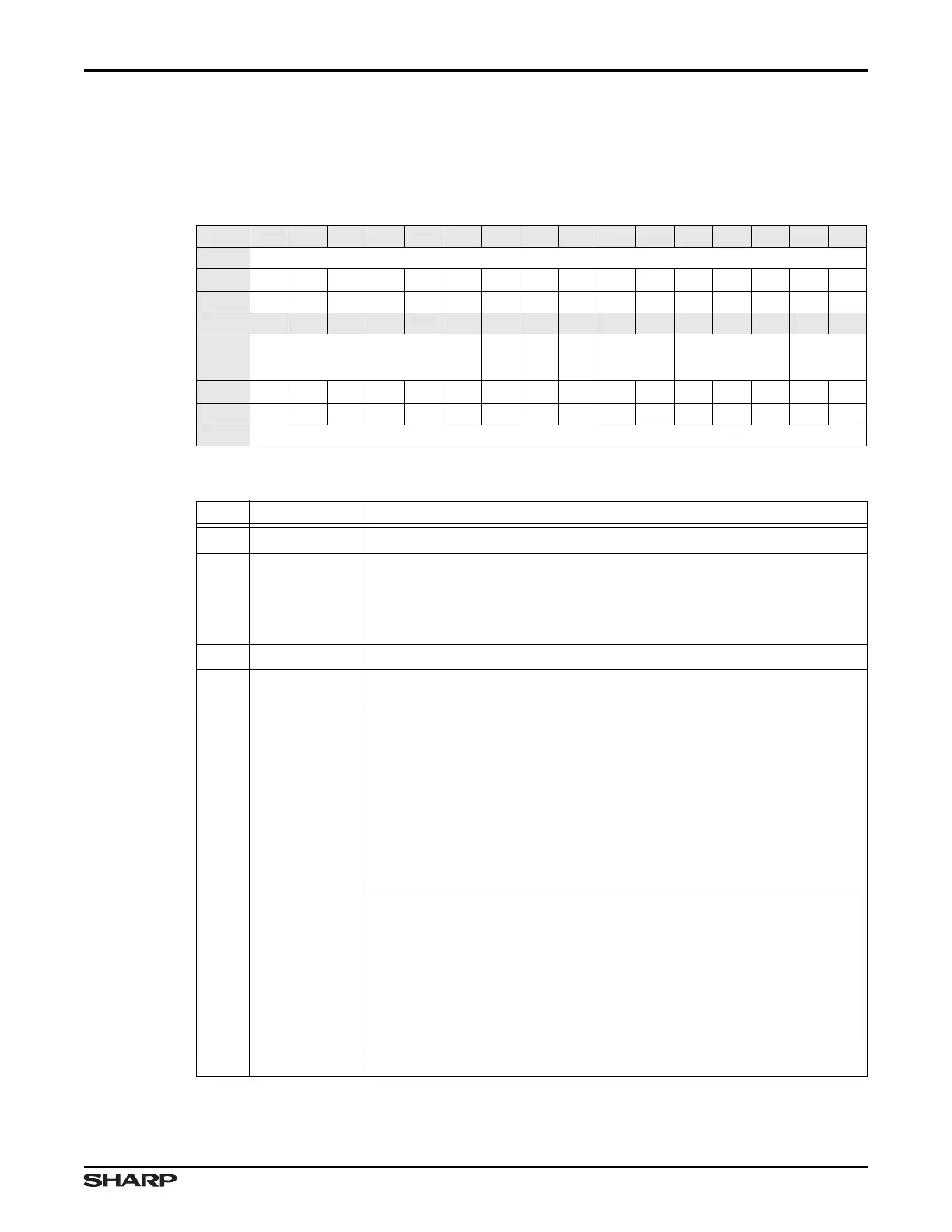
Table 13-4. CTRL Register
BIT 31 30 29 28 27 26 25 24 23 22 21 20 19 18 17 16
FIELD ///
RESET 0000000000000000
RW RO RO RO RO RO RO RO RO RO RO RO RO RO RO RO RO
BIT 15 14 13 12 11 10 9 8 7 6 5 4 3 2 1 0
FIELD ///
LOCK
/// /// OUTSEL PWRDWNSEL ///
RESET 0000001001100011
RW RO RO RO RO RO RO RW RO RW RW RW RW RW RW RW RW
ADDR 0xFFFE2000 + 0x00
Table 13-5. CTRL Fields
BITS NAME DESCRIPTION
31:10 /// Reserved Reading returns 0. Write the reset value.
9LOCK
Lock
0 = All RCPC registers that are accessible through the APB, other than
this bit and the INTCLR Register, are write protected.
1 = All RCPC APB-accessible registers are write enabled. (default)
8 /// Reserved Reading returns 0. Write the reset value.
7 ///
Reserved Read as 0. Always write 0. Writing a 1 causes unpredictable
results.
6:5 OUTSEL
CLKOUT Source Select Select the source clock for the CLKOUT
external clock pin.
00 = System Clock Oscillator (nominally 11.2896 MHz)
01 = Off*
10 = FCLK
11 = HCLK
*IMPORTANT: For A.0 silicon, selection 01 is an invalid value. For A.1
silicon, the output is held LOW.
4:2 PWRDWNSEL
Power Down Mode Select These bits always read 0b000 because
the RCPC clears them automatically at wakeup.
000 = Active Mode
001 = Standby Mode
010 = Sleep Mode
011 = Stop1 Mode
100 = Stop2 Mode
Other values = undefined.
1:0 /// Reserved Reading returns 1. Always write 1.