Color Liquid Crystal Display Controller LH79524/LH79525 User’s Guide
4-24 Version 1.0
4.5.3.3 Clock and Signal Polarity Control Register (TIMING2)
The TIMING2 Register controls the CLCDC timing.
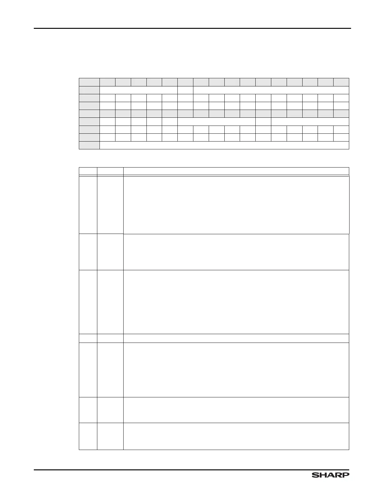
Table 4-18. TIMING2 Register
BIT 31 30 29 28 27 26 25 24 23 22 21 20 19 18 17 16
FIELD PCD_HI BCD CPL
RESET 0000000000000000
RW RW RW RW RW RW RW RW RW RW RW RW RW RW RW RW RW
BIT 15 14 13 12 11 10 9 8 7 6 5 4 3 2 1 0
FIELD /// IOE IPC IHS IVS ACB /// PCD_LO
RESET 0000000000000000
RW RO RW RW RW RW RW RW RW RW RW RO RW RW RW RW RW
ADDR 0xFFFF4000 + 0x08
Table 4-19. TIMING2 Fields
BIT NAME DESCRIPTION
31:27 PCD_HI
Panel Clock Divisor (upper five bits) The ten-bit PCD field, comprising PCD_HI
and PCD_LO (bits [4:0]) is used to derive the LCD Panel clock frequency CLCP from the
CLCDCLK frequency: CLCP = CLCDCLK/(PCD + 2).
For mono STN displays with a four or eight-bit interface, the panel clock is a factor of four
and eight of the actual individual pixel clock rate. For color STN displays, 2 2/3 pixels are
output per CLCP cycle, therefore the panel clock is 0.375 times.
For TFT displays the pixel clock divider can be bypassed by setting the TIMING2:BCD bit.
26 BCD
Bypass Pixel Clock Divider
1 = Bypass the pixel clock divider logic
0 = Use the pixel clock divider logic
See the description of the PCD bit field, below.
25:16 CPL
Clocks Per Line CPL specifies the number of LCDDCLK pulses fed to the LCD panel
during each horizontal line. The TIMING2:CPL and TIMING0:PPL fields work together;
both must be programmed correctly in order for the CLCDC to function correctly.
Actual Pixels Per Line (APPL) = 16 x (TIMING0:PPL – 1)
TFT panels: CPL = (APPL – 1)
4-bit mono STN panels: CPL = ((APPL/4) – 1)
8-bit mono STN panels: CPL = ((APPL/8) – 1)
Color STN panels: CPL = (((3 x APPL) / 8) – 1)
15
/// Reserved Reading returns 0. Write the reset value.
14 IOE
Invert Output Enable IOE applies only to TFT modes and should be programmed
to 0 for all other modes. In the TFT mode, the LCDEN pin indicates to the LCD panel that
valid display data is available. IOE selects the active polarity of this output enable signal.
In the TFT mode, data is driven onto the LCD data lines at the programmed edge of LCD-
DCLK when LCDEN is asserted.
1 = The LCDEN output pin is active LOW
0 = The LCDEN output pin is active HIGH
13 IPC
Invert Panel Clock IPC selects the active edge of the LCDDCLK signal.
1 = Data is driven on the LCD data lines on the falling-edge of LCDDCLK
0 = Data is driven on the LCD data lines on the rising-edge of LCDDCLK
12 IHS
Invert Horizontal Synchronization IHS selects the polarity of the LCDLP signal.
1 = The LCDLP pin is active LOW
0 = The LCDLP pin is active HIGH