External Memory Controller LH79524/LH79525 User’s Guide
7-48 Version 1.0
7.5.2.19 Dynamic Configuration Register for nDCS0
and nDCS1 (DYNCFGx)
The Dynamic Configuration Register specifies the configuration information for the rele-
vant dynamic memory Chip Select. These registers are normally only modified during sys-
tem initialization.
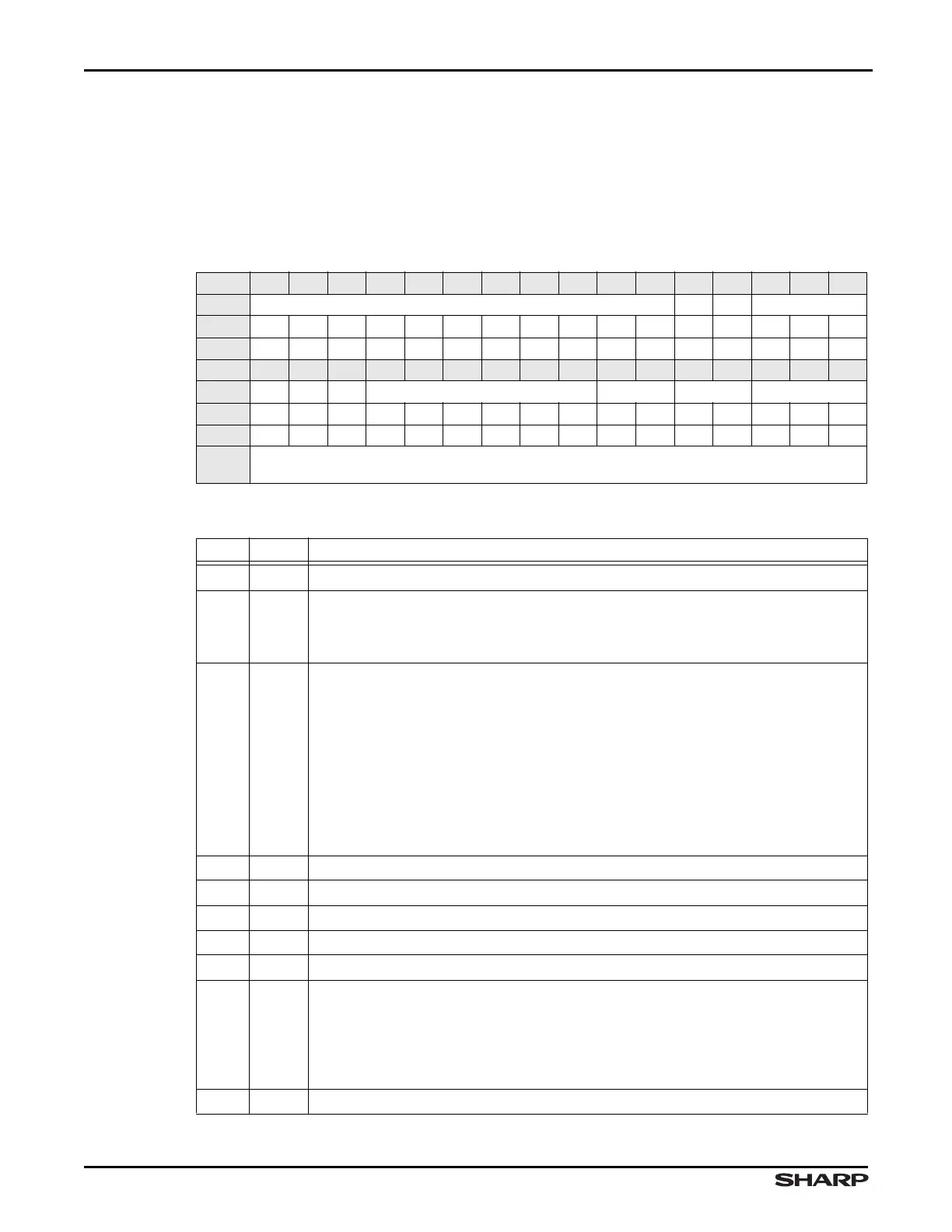
Table 7-47. DYNCFGx Register
BIT 31 30 29 28 27 26 25 24 23 22 21 20 19 18 17 16
FIELD ///
P
B ///
RESET 0000000000000000
TYPE RO RO RO RO RO RO RO RO RO RO RO RW RW RW RW RW
BIT 15 14 13 12 11 10 9 8 7 6 5 4 3 2 1 0
FIELD /// AM /// AM /// MD ///
RESET 0000000000000000
TYPE RW RW RW RW RW RW RW RW RW RW RW RW RW RW RW RW
ADDR
0xFFFF1000 + 0x100 for DYNCFG0
0xFFFF1000 + 0x120 for DYNCFG1
Table 7-48. DYNCFGx Fields
BITS NAME FUNCTION
31:21 /// Reserved Reading returns 0. Write the reset value.
20 P
Write Protect
1 = Write protected
0 = Not Write protected
19 B
Read and Write Buffer Enable The Buffer Enable bit must be set to 1 for prop-
er SDRAM interface operation. The buffers must be disabled during SDRAM and
SyncFlash initialization. They must also be disabled when performing SyncFlash
commands. The buffers must be enabled during normal operation.
NOTE: The buffers must be disabled during SDRAM and SyncFlash initializa-
tion, and when performing SyncFlash commands. The buffers must be enabled
during normal operation.
1 = Read and Write Buffers enabled for accesses to this Chip Select
0 = Read and Write Buffers disabled for accesses to this Chip Select
18:15 /// Reserved Read undefined, must write as zeros.
14 AM Address Mapping See Table 7-49
13 /// Reserved Read undefined, must write as zeros.
12:7 AM Address Mapping See Table 7-49
6:5 /// Reserved Read undefined, must write as zeros.
4:3 MD
Memory Device
00 = SDRAM
01 = low-power SDRAM
10 = Micron SyncFlash
11 = reserved
2:0 /// Reserved Read undefined, must write as zeros.