External Memory Controller LH79524/LH79525 User’s Guide
7-22 Version 1.0
7.4 Dynamic Memory
7.4.1 Write-protection
Each dynamic memory Chip Select can be configured for write-protection by setting the rel-
evant bit in the write-protect field in the DYNCFGx register (DYNCFGx:P). If a write access
is performed to a write-protected memory bank, an ERROR response is generated on the
HRESP[1:0] signal. For more information on HRESP see the ARM AMBA specification.
7.4.2 Access Sequencing and Memory Width
Configure the data width of each external Chip Select space by programming the appro-
priate DYNCFGx register. If the Chip Select data bus width is narrower than the request
from the current AMBA bus master, the internal bus transfer takes several external bus
transfers to complete. For example, if Chip Select 1 (nDCS1) is configured as 16-bit wide
memory and a 32-bit read is initiated, the AHB stalls while the EMC reads two consecutive
words from the memory. During these accesses the EMC demultiplexes the data into one
32-bit word and places it on the AHB. Word transfers are the widest transfers supported,
and access attempted with a size larger than a word generates an error response.
7.4.3 Bus Address Mapping
These tables provide the mapping of AHB address bus addresses to the external dynamic
memory address for various memory configurations and bus widths. The address mapping
is selected by programming the Address Mapping (AM) bits in the DYNCFGx register.
Note that Auto Precharge is always presented on A10 column address.
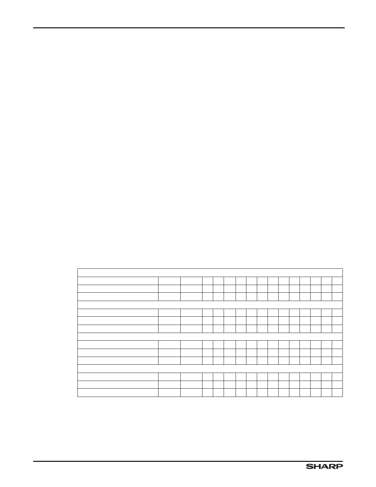
Table 7-5. 32-bit Wide Data Bus Address Mapping, SDRAM (RBC)
32-BIT DEVICE 16M SDRAM (1M × 16, RBC)
External Address Pin, A[14:0] 14 13 1211109876543210
AHB Address To Row Address — 10/BA0 — — 21 20 19 18 17 16 15 14 13 12 11
AHB Address To Column Address — 10/BA0——AP——98765432
32-BIT DEVICE 16M SDRAM (2M × 8, RBC)
External Address Pin, A[14:0] 14 13 1211109876543210
AHB Address To Row Address 11/BA1 — —— 2221201918171615141312
AHB Address To Column Address11/BA1 — ——AP—1098765432
32-BIT DEVICE 64M SDRAM (2M × 32, RBC)
External Address Pin, A[14:0] 14 13 1211109876543210
AHB Address To Row Address 11/BA1 10/BA0 — — 22 21 20 19 18 17 16 15 14 13 12
AHB Address To Column Address11/BA110/BA0——AP——98765432
32-BIT DEVICE 64M SDRAM (4M × 16, RBC)
External Address Pin, A[14:0] 14 13 1211109876543210
AHB Address To Row Address 11/BA1 10/BA0 — 23 22 21 20 19 18 17 16 15 14 13 12
AHB Address To Column Address11/BA110/BA0——AP——98765432