LH79524/LH79525 User’s Guide Reset, Clock, and Power Controller
Version 1.0 13-27
13.2.2.17 ADC Clock Prescaler Register (ADCPRE)
The value in this register is used as a divisor for the Source Clock to derive the ADC
clock (ADCCLK) frequency. The ACD clock source (System Clock Oscillator, or HCLK) is
selected with the PCLKSEL1:ADC bit (see Section 13.2.2.13). Following reset, the pres-
caler is programmed to pass the clock through without division. Table 13-42 shows the
valid combinations for ADCDIV and the resulting ADC clock frequency. All other ADCDIV
values are invalid.
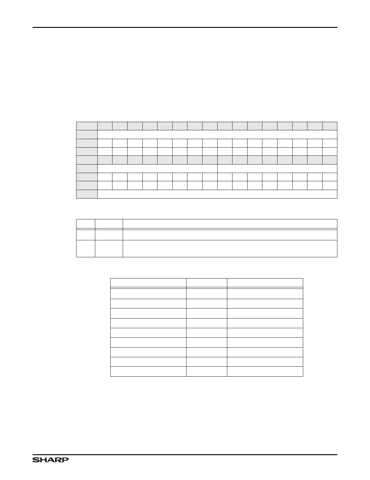
Table 13-40. ADCPRE Register
BIT 31 30 29 28 27 26 25 24 23 22 21 20 19 18 17 16
FIELD ///
RESET 0000000000000000
RW RO RO RO RO RO RO RO RO RO RO RO RO RO RO RO RO
BIT 15 14 13 12 11 10 9 8 7 6 5 4 3 2 1 0
FIELD /// ADCDIV
RESET 0000000000000000
RW RO RO RO RO RO RO RO RO RW RW RW RW RW RW RW RW
ADDR 0xFFFE2000 + 0x48
Table 13-41. ADCPRE Fields
BITS NAME DESCRIPTION
31:8 /// Reserved Reading returns 0. Write the reset value.
7:0 ADCDIV
ADC Clock Divisor Program with the clock source divisor for the ADC Clock
prescaler (see Table 13-42).
Table 13-42. ADCPRE Register Values
ADCDIV DIVISOR ƒ(ADCCLK)
0b00000000 (default) 1 ƒ(clock source)
0b00000001 2 ƒ(clock source)/2
0b00000010 4 ƒ(clock source)/4
0b00000100 8 ƒ(clock source)/8
0b00001000 16 ƒ(clock source)/16
0b00010000 32 ƒ(clock source)/32
0b00100000 64 ƒ(clock source)/64
0b01000000 128 ƒ(clock source)/128
0b10000000 256 ƒ(clock source)/256